Material Science and Engineering
Peel-apart surfaces drive transistors to the ledge
Surfaces featuring atomic-scale ledges and steps can act as reusable templates for producing nanoelectronic components.


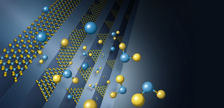
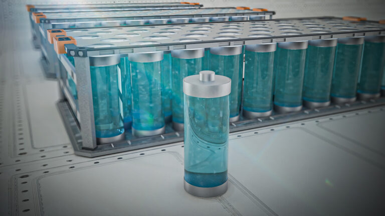
KAUST researchers are developing alternative approaches to TMD fabrication using surface templates to direct single-crystal growth. © 2020 KAUST
KAUST researchers are developing alternative approaches to TMD fabrication using surface templates to direct single-crystal growth. © 2020 KAUST
Semiconductor manufacturers are paying more attention to two-dimensional materials, such as transition metal dichalcogenides (TMDs), following the discovery at KAUST of an epitaxial growth process of single-crystal TMDs nanoribbons.
An emerging trend in transistor design involves space-saving architectures that stack components on top of one other. TMDs have potential for these systems because they readily form into thin sheets, known as nanoribbons, which have electrical, optical and magnetic activity. However, typical semiconductor processes, such as photolithography, require complicated procedures to produce TMDs of sufficient quality for device purposes.
In collaboration with researchers in the U.S., Belgium and Taiwan, Vincent Tung and colleagues at KAUST are developing alternative approaches to TMD fabrication using surface templates to direct single-crystal growth.
While analyzing candidates with high-resolution electron microscopy, researcher Areej Aljarb spotted something unusual about a semiconductor named gallium trioxide (Ga2O3). After peeling off layers of the flaky material using sticky tape, she saw arrays of narrow, terrace-like ledges that stepped up or down along the entire Ga2O3 surface.
“The steps are very steep and well exposed,” says Aljarb. “And because the atoms located near the vicinity of these ledges have asymmetric structures, they can drive growth in specific directions.”
When the team exposed Ga2O3 surfaces to a mix of molybdenum and sulfur gas, they observed that TMD nanoribbons crystallized lengthwise along the ledges with structures that were practically defect free. Microscopy experiments and theoretical models revealed that the ledge atoms had unique energetic features that enabled aligned nucleation to form single-crystal nanoribbons. “For decades, scientists have sought to grow 2D single-crystal semiconductors on insulators, and this work demonstrates that controlling the ledges of the substrate is the key,” says Tung.
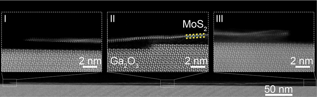
This cross-section view shows the long and monolayer MoS2 nanoribbon on top of the ledge of the Ga2O3 substrate.
© 2020 KAUST
Intriguingly, the nanoribbons could be pulled off and transferred to other substrates without damaging them. To explore potential applications of the ledge-directed growth technology, the international group joined together to design a transistor capable of incorporating nanoribbons from the Ga2O3 template. Electronic measurements showed the new transistor could operate at high speeds and had amplification factors similar to TMD materials produced through more labor-intensive techniques.
“The nanoribbons grow along the ledges using weak physical interactions to stay in place, meaning that no chemical bonds form between the TMD and the underlying Ga2O3 substrate,” notes Aljarb. “This unique feature enables us to transfer the nanoribbons onto foreign substrates for many applications, including transistors, sensors, artificial muscles and atomically thin photovoltaics.”
References
- Aljarb, A., Fu, J.-H., Hsu, C.-C., Chuu, C.-P., Wan, Y., Hakami, M., Naphade,D.R., Yengel, E., Lee, C.-J., Brems, S., Chen, T.-A., Li, M.-Y., Bae, S.-B., Hsu, W.-T., Cao, Z., Albaridy, R., Lopatin, S., Chang, W.-H., Anthopoulos, T.D., Kim, J., Li, L.-J. & Tung, V. Ledge-directed epitaxy of continuous, self-aligned and monolayer TMDs nanoribbons with single crystallinity. Nature Materials, 19 (2020).| article
ABOUT THE AUTHOR
Areej Aljarb
Ph.D. Student
You might also like
Applied Physics
Colorful solution to advanced disease diagnosis
Chemistry
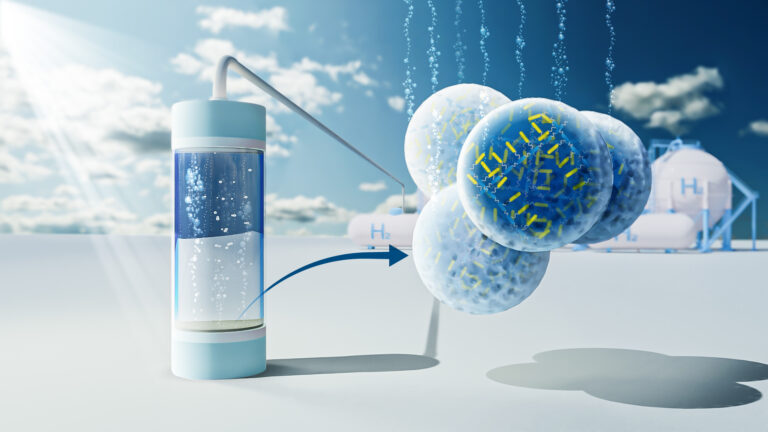
Turning infrared solar photons into hydrogen fuel
Applied Physics
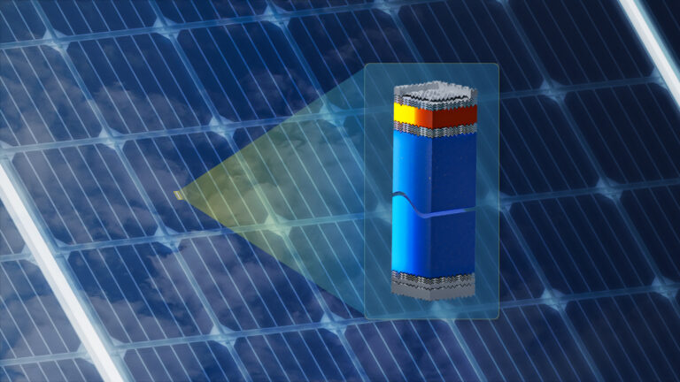
A single additive enables long-life, high-voltage sodium batteries

Bioengineering
Smart patch detects allergies before symptoms strike
Applied Physics
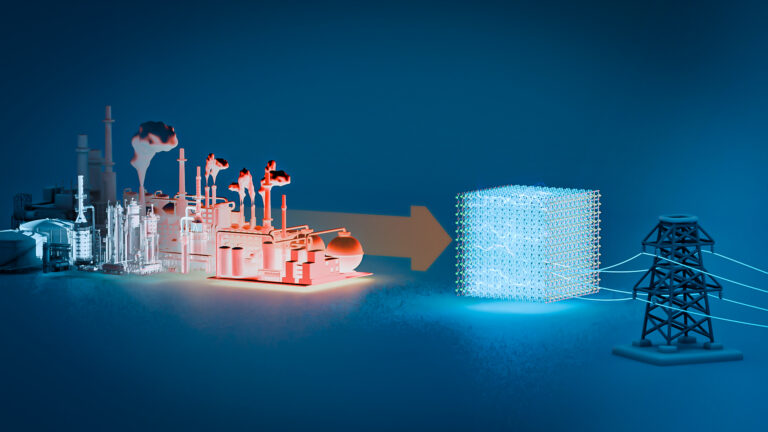
Two-dimensional altermagnets could power waste heat recovery
Applied Physics
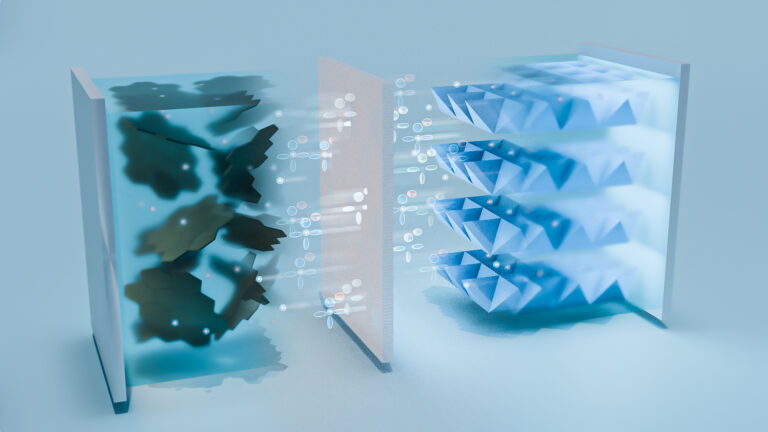
Interface engineering unlocks efficient, stable solar cells
Applied Physics
The right salt supercharges battery lifespan
Applied Physics