Applied Physics | Material Science and Engineering
Light-powered ‘smart vision’ memories take a leap forward
Broadband, reconfigurable photonic memristors set the stage for next-generation artificial vision systems.


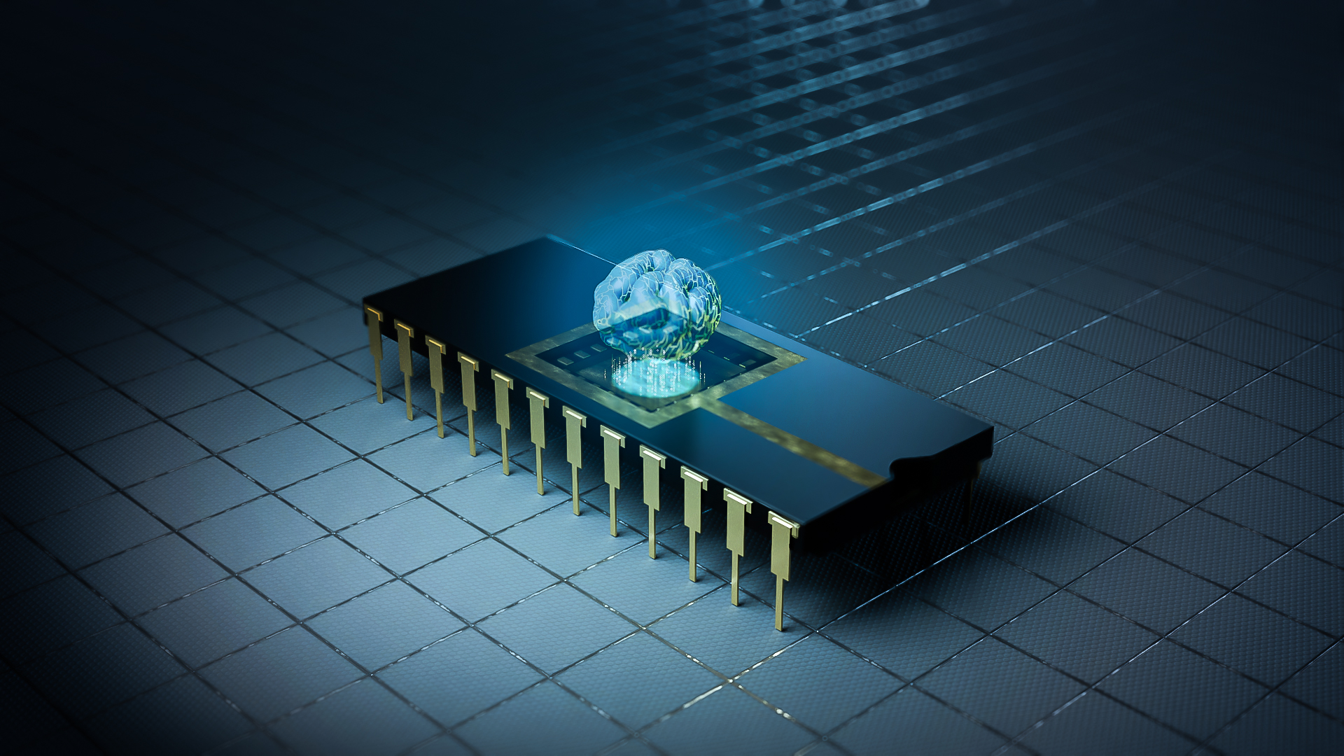
Artificial vision systems that combine image sensing, memory, and processing in one compact platform are a step closer to real-world application following a major advancement led by researchers at KAUST. The team has developed high-performance, light-controlled memory devices, or photonic memristors, that mark a significant step toward energy-efficient, integrated ‘smart vision’ hardware[1].
Memristors exhibit a resistance that varies with applied current flow and retain this resistance even when the current is turned off. Their ability to remember resistance based on past current flow enables memory and computation in one component, which is essential for data storage and neuromorphic computing. They display two distinct brain-like resistive switching modes: non-volatile and volatile modes, mimicking long-term and short-term memory, respectively.
Typically, memristors comprise metal-oxide thin films that respond to electrical stimuli but have several manufacturing challenges and performance limitations. Photonic memristors use light, a low-power, non-destructive, and contactless stimulus, to trigger switching, which provides a fast and energy-efficient alternative to conventional devices. The devices that contain atomically-thin two-dimensional materials, such as hexagonal boron nitride (hBN), feature excellent thermal stability, mechanical flexibility, and transparency. However, they are limited to narrow wavelength ranges and work in a single mode.
To harness hBN’s exceptional thermal stability and silicon’s light-absorption capabilities, an international team led by Maolin Chen, Xixiang Zhang, and with co-workers from KAUST have created photonic memristors by combining both materials in a layered arrangement.
The researchers produced uniform nanocrystalline hBN films using a low-temperature process called plasma-enhanced chemical vapor deposition to ensure compatibility with existing silicon-based manufacturing. They incorporated the films into memristor arrays on four-inch wafers, which is consistent with the scalability of the devices to industrial applications.
“Our memristors enable ‘all-in-one’ vision chips: they include image sensing, data storage, and parallel processing,” Chen says. In addition to high memory stability and durability, the devices exhibit a switching ratio exceeding one billion.
The memristors dynamically change their resistive switching behavior when exposed to different light conditions. They respond to a wide wavelength range from ultraviolet to near-infrared light, indicating compatibility with broadband operation.
They also achieve on-demand reconfigurability between memory modes using light intensity. They do not show any resistive switching in the dark but change from volatile to non-volatile modes when light intensity increases.
“Volatile and non-volatile switching mimics neuroplasticity, such as short-term adaptation versus long-term memory,” Chen says. This multi-mode behavior emulates how human visual neurons respond to stimuli of varying strength, which is crucial for artificial vision systems operating in dynamic environments.
The light-induced change arises from interactions between photogenerated electrons from the silicon layer and hydrogen ions migrating within the hBN layer. These interactions create tiny conductive paths, or filaments, which sets the resistance state. These filaments also form, persist, or vanish depending on how light interacts with the materials.
The researchers discovered that the filaments originate from the ionization of airborne water molecules under applied voltage. The electric fields dissociate the water molecules at the grain boundaries of hBN to yield the migrating hydrogen ions, Chen explains.
The team is working on scaling down devices for higher-density integration, implementing three-dimensional stacking for ultra-compact neuromorphic hardware, and testing in-memory computing for real-time AI vision tasks.
Reference
- Chen, M., Ma, Y., Aslam, N., Liu, C., Chen, Y., Luo, L., Zhang, X., Mai, K., Xiao, H., Zhu, K., Alharbi, O., Zheng, D. , Xu, X., Liao, H., Yang, Y., Wang, H., Zhou, Z., Wang, H., Tian, B., Li, J., He, X., Chang, K., Wan, Y., Shamim, A., Alshareef, H. N., Lanza, M., Anthopoulos, T. A., Han, Z., Xue, F. & Zhang, X. Ultrawide bandwidth boron nitride photonic memristors. Nature Nanotechnology (2025). | article.
ABOUT THE AUTHOR
Maolin Chen
Postdoc

You might also like

Applied Physics
Colorful solution to advanced disease diagnosis
Chemistry
Turning infrared solar photons into hydrogen fuel
Applied Physics
A single additive enables long-life, high-voltage sodium batteries
Bioengineering
Smart patch detects allergies before symptoms strike
Applied Physics
Two-dimensional altermagnets could power waste heat recovery
Applied Physics
Interface engineering unlocks efficient, stable solar cells
Applied Physics
The right salt supercharges battery lifespan
Applied Physics