Material Science and Engineering
Electron movie guides design of layered perovskite materials
Tracking how charge flows across the surfaces of 2D perovskites should help to design better solar cells and light-emitting diodes.


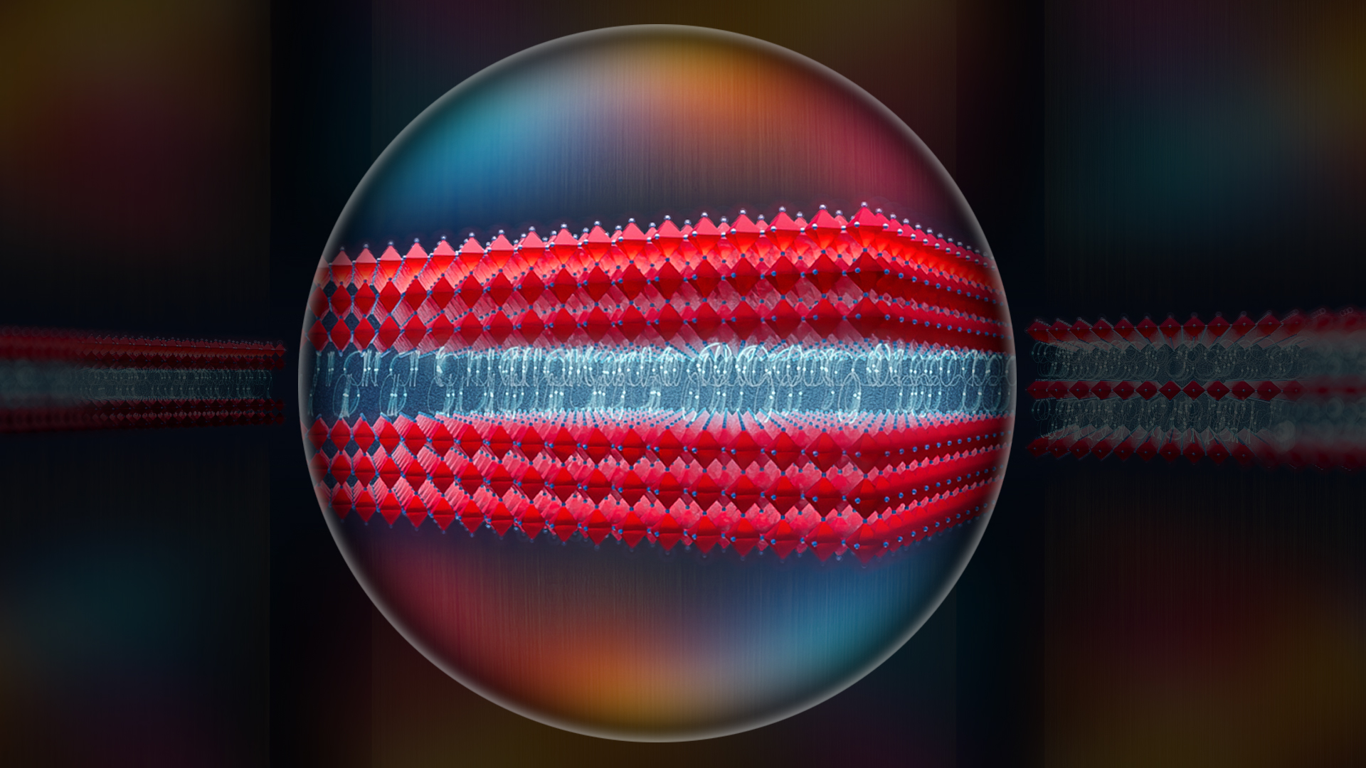
Detailed ‘movies’ that show how electrical charge flows through a layered material known as a 2D perovskite provide insights into how the perovskite could be fine-tuned to develop electronic devices that operate faster, last longer, and perform more efficiently[1].
“Researchers can use these results to carefully select the right number of layers and tailor surface chemistry to design improved 2D perovskite materials for applications such as solar cells and photodetectors,” says Lijie Wang from KAUST, part of the team behind the work.
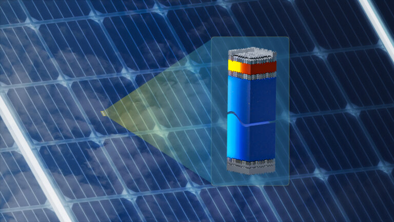
Perovskites can form thin crystalline films that convert light into electricity or vice versa. They are being commercialized in next-generation solar panels and show promise in applications such as light-emitting diodes (LEDs). Researchers make perovskites by combining inorganic materials like lead iodide with carbon-based organic molecules. However, exposure to heat, moisture, or intense light can degrade perovskites and their performance.
Researchers hope to solve these problems using closely related materials called 2D perovskites, in which the organic and inorganic components are arranged in alternating flat sheets, rather like a sandwich. The organic molecules serve as a barrier, preventing moisture and oxygen from reaching the inorganic slabs between them. “This structure significantly slows down the degradation processes and improves thermal stability,” says KAUST’s Omar Mohammed, who led the team.
In devices such as solar cells and LEDs, electrical charge is carried by negative electrons and the positive ‘holes’ they leave behind. The insulating organic components in 2D perovskites confine these charges to the inorganic slabs. While this can improve the efficiency of LEDs, it hinders the movement of charge in solar cells and photodetectors.
The KAUST team has now studied how the structure of 2D perovskites affects the behavior of electrons and holes using four-dimensional scanning ultrafast electron microscopy (4D-SUEM).
First, a laser pulse excites the perovskite, generating mobile electrons and holes that quickly spread out. An instant later, the microscope fires a pulse of electrons that bounce off the material and into a detector. Crucially, these pulse electrons are more readily reflected by parts of the sample with higher electron and hole densities.
By taking repeated snapshots of the perovskite in this way, the system creates a movie showing how the distribution of electrons and holes on the surface changes over mere quadrillionths of a second.
The team used this approach to study 2D perovskites with inorganic slabs, either one, two, or three layers thick. In samples with two or three layers, electrons and holes separated more easily, and the charges were more likely to move rapidly across the surface rather than through the bulk of the material. “Faster surface diffusion allows for more efficient charge collection in devices such as solar cells and photodetectors, leading to improved device performance,” explains Wang.
“The next stage of our research is to investigate how charge carriers behave under real-world conditions, such as high temperatures, intense illumination, or radiation — all conditions that devices might encounter in harsh environments,” adds Mohammed.
Reference
- Wang, L., Wu, W., Yang, J., Nughays, R., Zhou, Y., Ugur, E., Zhang, X., Shao, B., Wang, J.-X., Yin, J., De Wolf, S., Bakr, O.M. & Mohammed, O.F. Real-space imaging of photo-generated surface carrier transport in 2D perovskites. Light: Science & Applications 14, 124 (2025).| article
ABOUT THE AUTHOR
Lijie Wang
Postdoc

You might also like

Applied Physics
Colorful solution to advanced disease diagnosis
Chemistry
Turning infrared solar photons into hydrogen fuel
Applied Physics
A single additive enables long-life, high-voltage sodium batteries

Bioengineering
Smart patch detects allergies before symptoms strike
Applied Physics
Two-dimensional altermagnets could power waste heat recovery
Applied Physics
Interface engineering unlocks efficient, stable solar cells

Applied Physics
The right salt supercharges battery lifespan

Applied Physics