Chemistry
Looking both ways for new-style semiconductors
Introducing asymmetry across the two sides of atomically thin materials brings new opportunities in semiconductors.


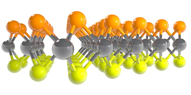
The uniquely asymmetric Janus monolayer has selenium atoms and sulfur atoms on different sides of the central plane of molybdenum atoms
© 2017 KAUST
Semiconductor materials called dichalcogenides may gain broader properties when asymmetry is introduced across the plane of sheets of bonded atoms.
KAUST researchers have created a Janus monolayer that, following Roman mythology, they named for Janus whose two faces looked in opposite directions and was believed to control transitions through gateways.
The Janus monolayers may help a transition to novel semiconductor applications in electronics, particularly in nanoelectronics, which relies on manipulating very small groups of atoms.
“Our unique method of synthesis paves the way for altering 2D, atomically thin sheets of these materials on an atomic scale,” says Lain-Jong Li, professor of chemical science.
Dichalcogenides are made when atoms from the transition-metal block in the periodic table combine with those from Group 16—the chalcogens. They have the general formula MX2, where M represents the transition metal and X represents the chalcogens. The KAUST researchers began with the symmetric material MoS2, with molybdenum (Mo) as the transition-metal atom and sulfur (S) as the chalcogen.
Their achievement was to selectively replace the sulfur atoms on one side of the atomically thin sheets with selenium atoms, creating their asymmetric Janus monolayer (see image). This is easy enough to describe, but was extremely difficult to perform. “It took us almost three years, step by step,” says Li.
It was worth the effort, Li explains, “because asymmetry introduces new properties.” In more technical terms, the key useful feature of semiconductor materials is that their electrons can occupy a range of energy levels or spin states. The asymmetry across the plane of a monolayer creates a richer diversity of energy levels, thus opening many more opportunities for use in real-world applications.
Li emphasizes that this research is still basic science; his team does not yet have any particular applications for the material, “but new physics and phenomena always emerge by discovering new materials,” he says.
In addition to conventional semiconductor applications, the researchers believe their asymmetric material could be useful in an emerging field called spintronics. This field uses changes in a property of electrons, known as their spin, rather than just their electric charge as a means of manipulating electronic behavior on atomically small scales.
Li now hopes to apply the innovation to other new Janus materials and thus widen the range of opportunities offered by introducing useful asymmetry.
References
- Lu, A-Y., Zhu, H., Xiao, J., Chuu, C-P., Han, Y., … & Li, L. Janus monolayers of transition metal dichalcogenides. Nature Nanotechnology 12, 744-749 (2017).| article
You might also like
Chemistry
Opening a window on architectural nano-design
Bioscience
Multi-enzyme pathway delivered into living cells

Chemical Engineering
Natural solvents enable fully bio-based membranes
Chemistry
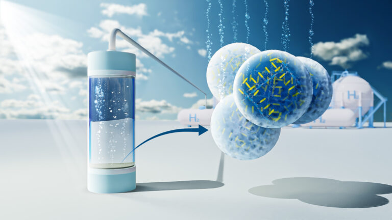
Turning infrared solar photons into hydrogen fuel
Applied Physics
Natural polymer boosts solar cells
Chemistry
Disruptive smart materials flex with real world potential
Chemistry
Catalysts provide the right pathway to green energy
Chemistry