Applied Physics
Phosphorus sets the pace in high-performance transistors
Ultrathin phosphorus semiconductors that become metallic when stacked can tackle resistance issues and boost transistor performance.


A newly discovered blue form of ultrathin phosphorus — with electronic properties that can be tuned to enhance the injection of charge carriers (negatively and positively charged) into transistors — are set to push next-generation electronic devices forward.
Two-dimensional semiconductors, such as graphene and transition metal dichalcogenides, are expected to drive the miniaturization of electronic devices by providing ultrathin active channels for charge-carrier transport in field effect transistors (FETs).
Essential to modern circuitry, FETs are used to influence the flow of current through their channels by applied voltage and behave like electronically controlled switches or amplifiers. However, electric resistance arises at the interfaces between the semiconductor channels and metal electrodes. This limits the charge injection into the devices and prevents the FETs from reaching their full potential.
“Reducing this contact resistance will improve the current delivery capability and improve the performance of the FETs, which will pave the way for future microelectronics,” says Shubham Tyagi, a Ph.D. student in Udo Schwingenschlögl’s group.
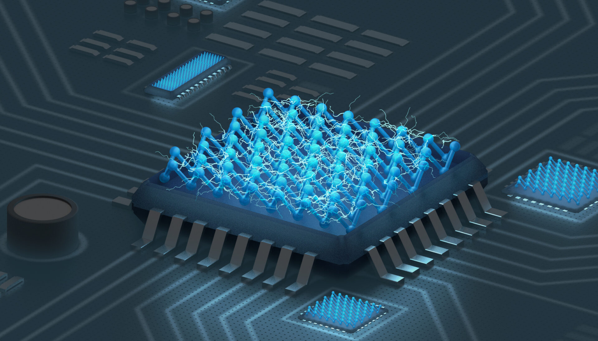
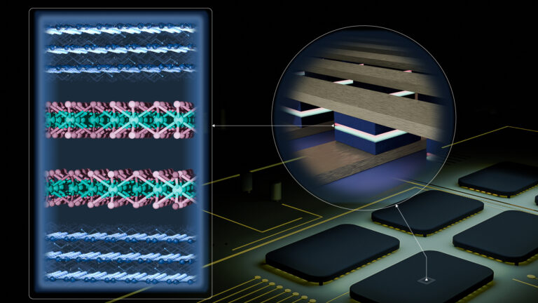
Now, Schwingenschlögl’s team has designed a junction-free FET using the recently discovered two-dimensional blue phosphorene as the single electroactive material.[1] Blue phosphorene itself is a semiconductor but becomes a metal when stacked into a bilayer.
“The ability of blue phosphorene to change its electronic properties based on stacking is crucial for our device,” Tyagi says. “Once we obtained a crystal orientation that delivers high carrier mobility through the channel, we were confident that we would achieve positive results because the contact resistance is addressed by the junction-free design,” he adds.
At the heart of the junction-free device is a blue phosphorene monolayer that, acting as the channel, lies between two metallic blue phosphorene bilayers that work as electrodes. The channel and electrodes consist of the same material, which results in a continuous structure, therefore reducing the resistance.
Using computer simulations, the researchers investigated the quantum transport in the proposed FET design for two different directions: armchair and zigzag. In both configurations, the FET effectively mediated electron transfer between channel and electrodes while meeting switching and amplification criteria. It outperformed devices using other two-dimensional materials, such as black phosphorene and monolayer molybdenum disulfide.
“In the future, we want to address different ways of improving the FET performance,” Tyagi says.
The researchers are working to reduce the current leakage between transistor gate and electrodes using van der Waals materials, which consist of sheets held together through weak interactions. They are also exploring ways to extend their ideas to magnetic materials to develop spintronic devices.
Reference
- Tyagi, S., Rout, P. C. & Schwingenschögl, U. High-performance junction-free field-effect transistor based on blue phosphorene. npj 2D Materials and Applications 6, 86 (2022).| article
ABOUT THE AUTHOR
Shubham Tyagi
Ph.D. Student

You might also like

Applied Physics
Colorful solution to advanced disease diagnosis
Applied Physics
A single additive enables long-life, high-voltage sodium batteries
Applied Physics
Two-dimensional altermagnets could power waste heat recovery
Applied Physics
Interface engineering unlocks efficient, stable solar cells
Applied Physics
The right salt supercharges battery lifespan
Applied Physics
Light-powered ‘smart vision’ memories take a leap forward
Applied Physics
Natural polymer boosts solar cells
Applied Physics