Chemistry
Microscope tracks carriers in space and time
An electron microscope fitted with a femtosecond laser visualizes the dynamics of excited carriers on the surface of a material in real space and time.


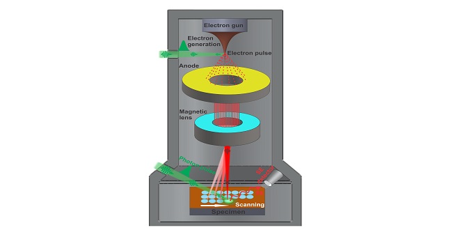
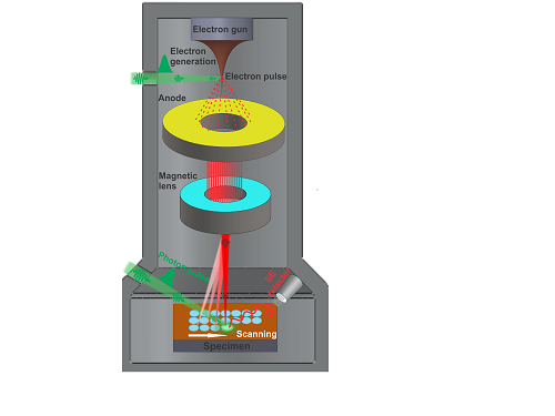
A four-dimensional ultrafast electron microscope enables ultrafast and high spatial resolution imaging of excited electrons on a surface.
© 2015 KAUST
Excited carriers on the surface of a material can behave very differently from those moving deeper within the material. KAUST researchers have demonstrated that these surface dynamics can be captured using the ultrafast and high spatial resolution technique of so-called four-dimensional ultrafast electron microscopy (4D UEM)1.
Understanding the dynamics of surface electrons and their positively-charged counter parts called holes is particularly important for optimizing electronic and electrochemical devices. For example, knowing how electrons and holes move to or from the surface of the catalyst can improve reactions that generate hydrogen from water.
Assistant Professor Omar Mohammed and his co-workers from the KAUST Solar and Photovoltaics Engineering Research Center have developed a form of microscopy able to visualize charge carrier dynamics with a high spatial resolution. The resolution was as clear as approximately 5 nanometers (5 × 10⁻⁹ meters) and a temporal resolution of 650 femtoseconds (650 × 10 12 seconds).
“The idea behind 4D electron imaging is to see dynamical processes with our own eyes in space and time,” said Mohammed.
The team’s technique uses a modified scanning electron microscope — a device that creates an image by sweeping a primary beam of electrons across the surface of the sample — and then detecting those that are scattered.
Mohammed and his colleagues integrated a high-power laser into their scanning electron microscope (SEM) to establish the second generation of 4D UEM in scanning mode. Femtosecond pulses of infrared light from this laser were split into two. The wavelength of one part was converted to green light and focused on the sample surface for dynamics initiation.
The other part of the laser was converted to an ultraviolet or green pulse and directed at a metallic tip. This generated a beam of pulsed electrons required for imaging. These electrons interacted with those excited on the surface of the sample and were either backscattered or produced further electrons, all of which were measured by a detector.
Imaging the changing charge-carrier dynamics in time was possible by varying the delay between the sample-surface exciting pulse and the pulse hitting the metal tip.
“Using pulsed electrons rather than the continuous electron beam used in conventional electron microscopy means that much faster changes can be captured,” explained Mohammed.
The researchers used their method to show how the shape of the surface and the presence of defects and nanometer-sized grains can significantly affect photo-induced processes.
“We can use this technique to image the movement of charged particles at interfaces in solar cells and optoelectronic devices, which until recently was a far-off-dream,” Mohammed added.
References
- Sun, J., Melnikov, V. A., Khan, J. I. & Mohammed, O. F. Real-space imaging of carrier dynamics of materials surfaces by second-generation four-dimensional scanning ultrafast electron microscopy. The Journal of Physical Chemistry Letters 6, 3884–3890 (2015).| article
You might also like

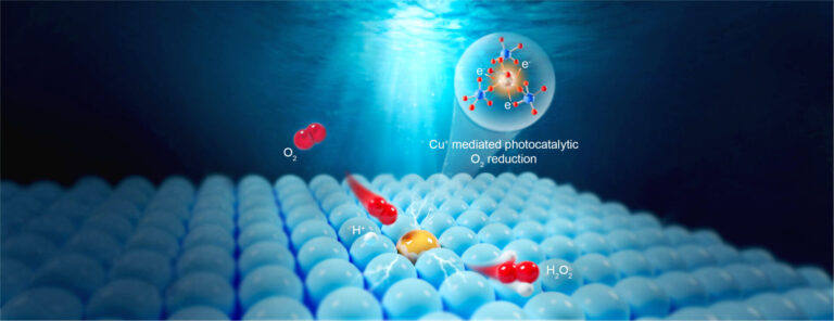
Chemical Engineering
Natural solvents enable fully bio-based membranes

Chemistry
Turning infrared solar photons into hydrogen fuel
Applied Physics
Natural polymer boosts solar cells
Chemistry
Disruptive smart materials flex with real world potential
Chemistry
Catalysts provide the right pathway to green energy
Chemistry
Hollow molecules offer sustainable hydrocarbon separation
Chemistry
Maximizing methane

Chemistry