Material Science and Engineering
Building approach for optoelectronics stacks up
A precise method for stacking semiconductor thin films enhances optoelectronic device performance using quantum effects.


KAUST core labs experts worked with researchers in Osman Bakr’s research group to develop a thermal evaporation technique.
© KAUST 2019
A method to nanoengineer an emerging family of semiconductors known as perovskites could reduce the cost of high-performance optoelectronic devices.
The properties of a semiconductor can be controlled by nanoscale engineering using technologies that slowly deposit atoms on a substrate. These methods are expensive and limited to conventional semiconductor materials, motivating scientists to search for new methods.
Quantum wells are semiconductor films of just a few nanometers, sandwiched between two thicker layers of a different semiconducting material. An energy barrier between the two materials blocks the electrical charge carriers from leaving the well layer, effectively limiting their motion to two dimensions. This radically alters the well material’s properties, making them more optically active, for example. This effect can be amplified further by combining multiple quantum wells into a single stack.
A bulk perovskite single crystal (right) becomes multiple quantum wells on a glass substrate (left) using the thermal-evaporation technique.
© 2019 KAUST
Epitaxial methods—depositing crystalline film on a crystalline substrate—are used to construct such stacks from gallium arsenide or gallium nitride by expensive processes with specialized equipment. But, another more practical approach is needed if this multiple quantum well architecture is to be used in perovskite devices. “Metal halide perovskites have excellent energy conversion efficiency for light harvesting and photoluminescence,” says postdoc Kwang Jae Lee from Osman Bakr’s Lab in the KAUST Catalyst Center. Quantum wells could improve this efficiency still further.
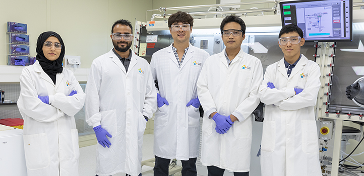
KAUST authors (l-r): Noor Merdad, Partha Maity, Kwang Jae Lee, Lutfan Sinatra, and Ayan A. Zhumekenov.
© 2019 KAUST
Working with colleagues from across KAUST and in collaboration with researchers from Korea, Bakr, Lee and team created perovskite multiple quantum wells using a simple technique known as thermal evaporation. They started with powders of their chosen perovskite well material, CsPbBr3, and a barrier material, TPBi. These powders evaporated when heated in a vacuum chamber, and the vapor particles traveled to a substrate where they formed a film. The team alternated between heating the TPBi and the CsPbBr3 to make their quantum wells.
Key to their success was calibration of the deposition rate. The team optimized the evaporation rates of their CsPbBr3 and TPBi powders at 0.015 and 0.020 nanometers per second, respectively. Unlike most epitaxial technologies, thermal evaporators are simple and widely available. Moreover, epitaxial methods need a substrate with a similar atomic lattice spacing to that of the deposited layer. The evaporation method, however, is applicable to any substrate; Lee and the team used simple glass because of the defect tolerance of perovskite materials.
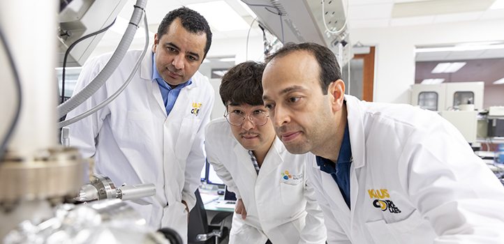
Kwang Jae Lee received support from KAUST’s Imaging and Characterization Core Lab to analyze the multiple quantum-well structure. Here, Mohamed N. Hedhili (left), Kwang Jae Lee and Nimber Wehbe operate a secondary ion-mass spectroscopy microscope used to scan the elemental distribution through the depth of the stacked structure.
© 2019 KAUST
“I think this is just the beginning,” says Lee. “The study points in one unexplored direction in perovskite research, and we expect further exciting perovskite devices based on this work in the near future.”
References
-
Lee, K. J, Turedi, B., Sinatra, L., Zhumekenov, A. A. Maity, P. Dursun, I., Naphade, R., Merdad, N., Alsalloum, A., Oh, S., Wehbe, N., Hedhill, M., Kang, C.H., Subedi, R.C., Cho, N., Kim, J.S., Ooi, B., Mohammed, O.F. & Bakr, O.M. Perovskite-based artificial multiple quantum wells. Nano Letters 6, 3535-3542 (2019).| article
ABOUT THE AUTHOR
Postdoc
Kwang Jae Lee

You might also like
Applied Physics
Colorful solution to advanced disease diagnosis
Chemistry
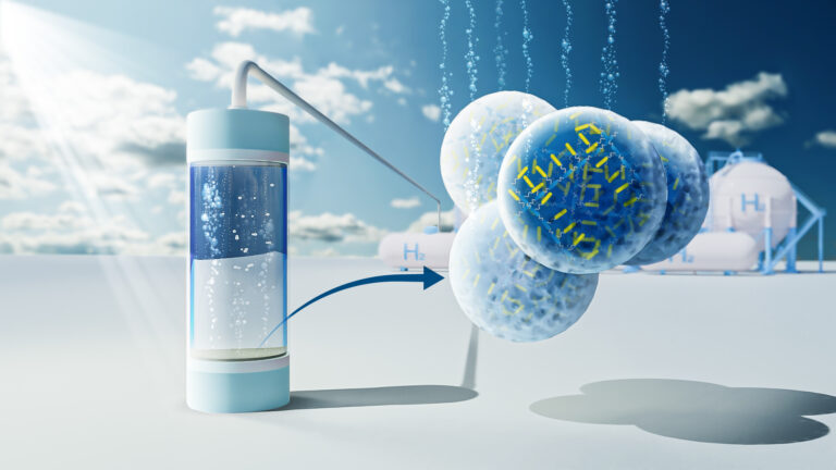
Turning infrared solar photons into hydrogen fuel
Applied Physics
A single additive enables long-life, high-voltage sodium batteries

Bioengineering
Smart patch detects allergies before symptoms strike
Applied Physics
Two-dimensional altermagnets could power waste heat recovery
Applied Physics
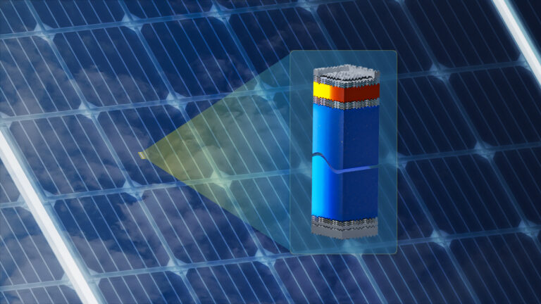
Interface engineering unlocks efficient, stable solar cells
Applied Physics
The right salt supercharges battery lifespan

Applied Physics