Material Science and Engineering
Atom-thin insulator grown into perfect films
Hexagons of hexagonal boron nitride join up to form two-dimensional insulator for next-generation electronic devices.
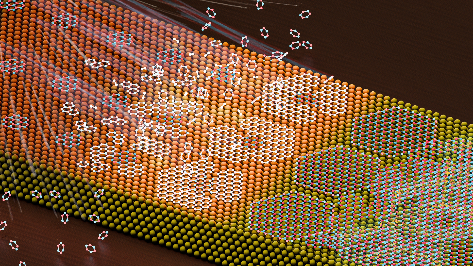
A method that can grow a useful insulating material into exceptionally high-quality films that are just one atom thick and is suitable for industrial-scale production has been developed by an international team led by Xixiang Zhang from KAUST[1].
The material, called hexagonal boron nitride (hBN), is used in semiconductor devices and can also enhance the performance of other two-dimensional (2D) materials such as graphene and transition metal dichalcogenides (TMDs).
Researchers can combine 2D materials to build tiny electronic components for quantum computing, electronic communications and other applications. While most 2D materials conduct electricity, hBN is one of the few that is an insulator, making it an indispensable component within many of these devices.
In the laboratory, hBN flakes are often peeled from bulk samples of the material, a time-consuming and size-limiting approach that is unsuitable for mass manufacturing. Alternatively, an industrial process called chemical vapor deposition (CVD) can produce hBN by decomposing a precursor called ammonia borane. Boron and nitrogen atoms released from the precursor then form triangular islands of hBN on a copper foil, and these islands gradually grow larger until they join together into a continuous honeycomb lattice.
The team has improved this process by growing hBN from hexagonal islands instead, producing a higher-quality film. “Hexagonal islands have fewer defects, making the final film more uniform and reliable,” says Zhang. The method depends on adding a trace of oxygen during the growth process.
As hBN islands grow on copper, their edges can be zigzags of either boron or nitrogen atoms. In the triangular islands, all three edges feature nitrogen atoms. In contrast, the hexagonal islands formed by the new method have three nitrogen edges and three boron edges.
The researchers’ theoretical calculations show that nitrogen edges are usually more energetically stable than boron edges, explaining why triangular islands are formed during CVD. But oxygen interacts with the islands and the copper foil in a way that gives the nitrogen and boron edges almost identical stabilities. This means the two types of edges can grow at the same rate, which generates hexagonal islands.
The researchers used techniques such as atomic force microscopy and high-resolution transmission electron microscopy to study the islands and films formed by their method. They found that it creates single-crystal films of hBN that are free of pinholes, exhibit low defect densities, have a uniform thickness, and possess excellent insulating properties. “This makes it especially suitable for high-performance 2D-material electronic devices and offers enhanced robustness for nanodevices,” says Bo Tian, who was part of the KAUST team, and is now based at Nanyang Technological University in Singapore.
The team used the method to grow a 25 x 70 mm film of hBN, and larger areas should be possible. “The process is now limited by the CVD system or substrate size, so it is suitable for industrial production,” Tian says. The researchers are now studying the mechanism of CVD growth of hBN in more detail, to further improve the quality and increase the size of the films they can produce.
Reference
- Li, J., Samad, A., Yuan, Y., Wang, Q., Hedhili, M. N., Lanza, M., Schwingenschlögl, U., Abate, I., Akinwande, D., Liu, Z., Tian, B. & Zhang, X. Single-crystal hBN monolayers from aligned hexagonal islands. Nature Communications 15, 8589 (2024).| article
You might also like
Chemistry
Turning infrared solar photons into hydrogen fuel

Applied Physics
A single additive enables long-life, high-voltage sodium batteries

Bioengineering
Smart patch detects allergies before symptoms strike

Applied Physics
Two-dimensional altermagnets could power waste heat recovery
Applied Physics
Interface engineering unlocks efficient, stable solar cells
Applied Physics
The right salt supercharges battery lifespan

Applied Physics
Light-powered ‘smart vision’ memories take a leap forward
Applied Physics


