Material Science and Engineering
Bending the norm on nanowires
Arranging nanowires in bent configurations may make them less likely to fail inside electronic devices.


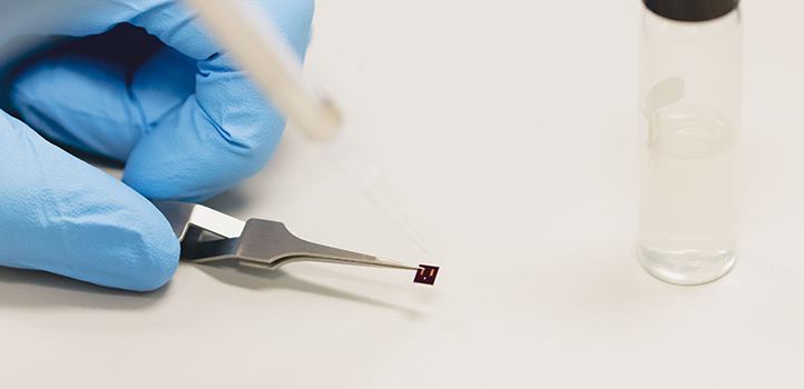
Nitin Batra and Pedro Costa worked with Ahad Syed of the Nanofabrication Core Lab to develop bent nanowires that are more resistant to strain than straight nanowires.
© 2019 KAUST
New methods of arranging silver nanowires make them more durable, shows a study by KAUST. These nanowires form flexible, transparent conductive layers that can be used for improved solar cells, strain sensors and next-generation mobile phones.
Applying nanotechnology in electronic devices requires rigorous testing of individual tiny components to ensure that they will stand up to use. Silver nanowires show great promise as connectors that could be arranged in flexible, near-transparent meshes for touchscreens or solar cells, but it is unclear how they will respond to prolonged stresses from bending and carrying current.
Testing the bulk properties of a large sample of nanoparticles is easy, but not completely revelatory. However, adopting transmission electron microscopy (TEM) makes it possible to examine individual nanoparticles. Ph.D. student Nitin Batra and his supervisor Pedro Costa are at the forefront of developing new TEM techniques. This has allowed them to study single silver nanowires in detail1.

Researchers load a sample of their bent nanowires into the TEM for analysis. (l-r): Nitin Batra, Ahad Syed and Pedro Costa.
© 2019 KAUST
“A major part of our work has been designing and fabricating sample platform prototypes (or ‘chips’) for TEM, which allow us to characterize and manipulate nanomaterials with an unsurpassed spatial resolution,” says Batra.
To improve on expensive commercially available chips that contain a very fragile membrane to support nanoparticles, Batra and Costa, with help from Ahad Syed of the Nanofabrication Core Lab at KAUST, have now submitted to patenting2 their own robust, reusable chips that do not require a membrane.
The researchers suspended silver nanowires from platinum electrodes over their custom-made TEM chips and applied a range of voltages until the nanowires failed due to heating by the electrical current. They found that straight nanowires tended to snap when they reached a certain high current density, at points determined by local structural defects.

Nitin Batra prepares a sample of nanowires to analyze using the NMR.
© 2019 KAUST
More interesting behavior was seen when the nanowires were bent from the beginning. These samples tended to buckle instead of snapping at high voltage and exhibited an ability to self-heal because they remained held together by the carbon coating on the outside of the wires. Some nanowires even exhibited resonant vibrations, like the harmonics on a guitar string, before they failed.
“Many devices are expected to undergo repeated bending and twisting by the end-user, which means that it is not realistic to limit the study of the electrical response of silver nanowires to straight configurations,” says Batra. “Our results suggest that the failure rate of such devices could be minimized by using bent nanowires instead of straight ones. The self-healing capability could effectively delay the breakdown of the circuit.”
References
-
Batra, N.M., Syed, A. & Costa, P.M.F.J. Current-induced restructuring in bent silver nanowires. Nanoscale 11, 3606-3618 (2019).| article
- US provisional patent 62/677,333. Patentees: Nitin M. Batra, Pedro M.F.J. Costa. Title “Membraneless platform for correlated analysis of nanomaterials” (2019).
ABOUT THE AUTHOR
Nitin Batra
Ph.D. Student

You might also like

Chemistry
Turning infrared solar photons into hydrogen fuel
Applied Physics
A single additive enables long-life, high-voltage sodium batteries
Bioengineering
Smart patch detects allergies before symptoms strike
Applied Physics
Two-dimensional altermagnets could power waste heat recovery
Applied Physics
Interface engineering unlocks efficient, stable solar cells
Applied Physics
The right salt supercharges battery lifespan

Applied Physics
Light-powered ‘smart vision’ memories take a leap forward
Applied Physics