Material Science and Engineering
Copper nanoclusters shape up
Atomically precise nanocluster may provide fresh direction for nanocatalysts.
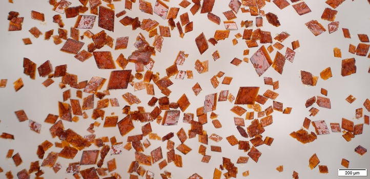
A unique nanocluster of copper atoms created by KAUST researchers could serve as a roadmap to guide the design of new catalysts and imaging agents.
A nanocluster is a type of nanoparticle in which researchers have pinpointed the precise arrangement of every atom, along with their bond lengths and bond angles. This detailed information enables researchers to predict the properties of related clusters, based on their composition and structures. “It provides a practical model for understanding the intrinsic correlations between structure and physical-chemical properties through a combination of experiments and theoretical calculations,” says Ren-Wu Huang of the KAUST Catalysis Center, part of the team behind the new discovery.
Nanoclusters are typically 1–3 nanometers wide and organized into a core and a shell. The atomic structure of the core can determine the nanocluster’s structure, size and optical properties, while the shell affects its stability, solubility and catalytic activity.
Nanoclusters containing copper, silver and gold have potential uses as catalysts, or as nontoxic luminescent imaging agents in living cells. Although silver and gold nanoclusters are well studied, copper nanoclusters have been rather neglected, partly because the metal tends to react with oxygen in air.
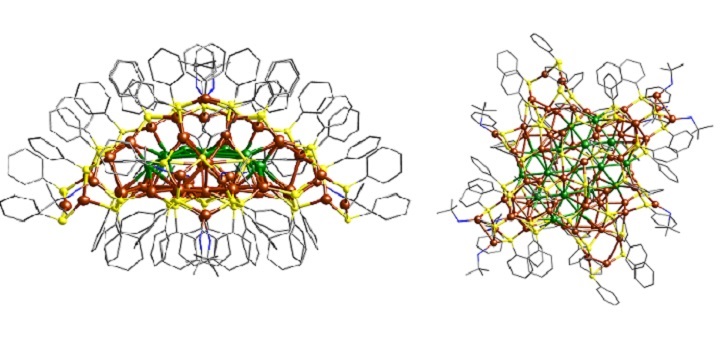
The side (left) and top (right) views of the nanocluster reveal that it is a flat core of 17 copper atoms (green). The cluster has 64 more copper atoms in its shell (brown), along with molecules containing sulfur (yellow), nitrogen (blue) and carbon (grey). Hydrogen atoms are omitted for clarity.
Reproduced with permission from reference one © 2020 Journal of the American Chemical Society.
The KAUST team has now created the largest copper-based nanocluster to date, and they are studying it with a range of techniques, including X-ray crystallography and electrospray ionization mass spectrometry. Each 2.8-nanometer-wide cluster contains 81 copper atoms, 46 benzenethiol molecules, 10 tert-butylamine molecules and 32 hydride ions.
Nanoclusters generally have polyhedral cores surrounded by symmetrical shells. But the new copper nanocluster has a flat core of 17 copper atoms, arranged into a repeating pattern of triangles. “This kind of planar core has never been observed in previously reported metal nanoclusters,” says Osman M. Bakr, who led the team.
The nanocluster also has a highly unusual hemispherical shell that is 1.5-nanometers high and covered by benzenethiol molecules. Differences between the curved and flat surfaces of the hemisphere suggest that the flat face has a higher reactivity. In addition, computational calculations provided evidence that the arrangement of these molecules could help to ease the transfer of electrical charge between different clusters within a crystal, which could prove crucial in future applications.
“The development of copper nanoclusters is still in its infancy,” says Huang. “Therefore, the next stage of our research will be the synthesis of copper nanoclusters with a bigger size and novel structure, and exploring their potential applications in the field of catalysis.”
References
-
Huang, R.-W., Yin, J., Dong, C., Ghosh, A., Alhilaly, M.J., Dong, X., Hedhili, M.N., Abou-Hamad, E., Alamer, B., Nematulloev, S., Han, Y., Mohammed, O.F. & Bakr, O.M. [Cu81(PhS)46(tBuNH2)10(H)32]3+ reveals the coexistence of large planar cores and hemispherical shells in high-nuclearity copper nanoclusters. Journal of the American Chemical Society 142, 8696−8705 (2020).| article
You might also like

Chemistry
Turning infrared solar photons into hydrogen fuel
Applied Physics
A single additive enables long-life, high-voltage sodium batteries

Bioengineering
Smart patch detects allergies before symptoms strike

Applied Physics
Two-dimensional altermagnets could power waste heat recovery
Applied Physics
Interface engineering unlocks efficient, stable solar cells
Applied Physics
The right salt supercharges battery lifespan

Applied Physics
Light-powered ‘smart vision’ memories take a leap forward
Applied Physics


