Material Science and Engineering
Sharpening up on core capabilities
Scientists working in KAUST’s Core Lab facilities are continuing to push the boundaries of what the university’s major instruments can do.


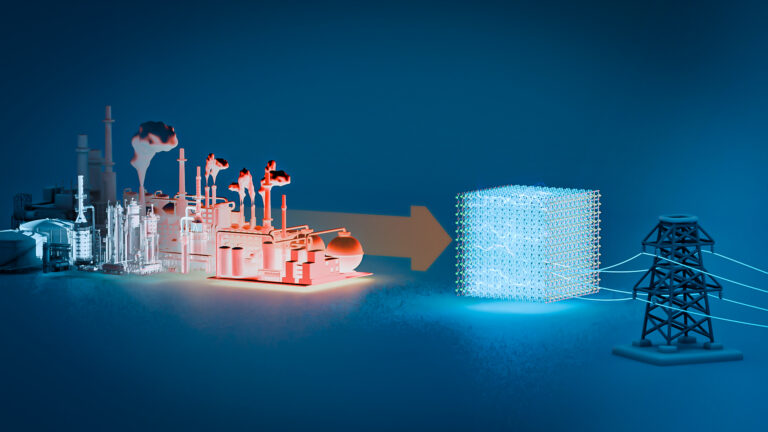
A technique for extracting sharper signals from an electron microscope, developed in the KAUST Core Laboratories, is offering unprecedented insights into the electronic properties of new materials created by the university’s researchers. The technique has already led to improvements in organic solar cell formulation and has revealed some extraordinary electronic properties of two-dimensional materials called MXenes.
For scientists working in the Core Labs, their role is to ensure that the major scientific equipment runs well and is available for use by researchers from KAUST, as well as across Saudi Arabia. Sometimes, the scientists are more hands on. “Where the required analysis goes beyond the capabilities of a regular user, we can offer extra help,” explains Sergei Lopatin, a Core Labs senior scientist, who specializes in electron microscopy.
Core Lab scientists can also apply for time on the machines they operate to test ideas for improving their performance. “We can then develop our own methods on the equipment, if it can benefit KAUST users,” Lopatin says. A recent idea Lopatin tested, for example, has turned out to be time well spent.
Electron microscopes can interrogate a sample’s electronic properties using a technique called electron energy loss spectroscopy (EELS). In the microscope, electrons are fired through the material. “As the electrons go through the sample, they interact with it and lose some of their energy,” Lopatin explains. “We can analyze how much energy they lose, to measure certain properties.”
To maximize the accuracy of the measurement, all the electrons fired through the sample would ideally start with exactly the same amount of energy. Electron microscopes are fitted with a kind of filter, called a monochromator, which enables the user to select electrons of a very narrow energy window. By tuning various monochromator parameters, Lopatin was able to show that he could narrow that window even further. “I managed to make it work five times better than the performance declared by the manufacturer,” Lopatin says.
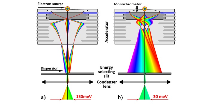
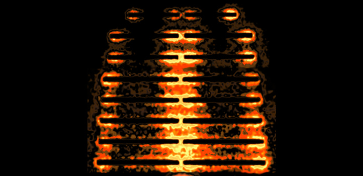
By adjusting the parameters of the monochromator, electrons of different energy (from high energy (purple) to low energy (red)) spread out more broadly (right), so that only electrons of a narrow energy window passed through the slit to be used in the experiment.
© 2020 Sergei Lopatin
The opportunity to use the new technique soon arose. “By good coincidence, a student came to me with a new material to test,” Lopatin says. KAUST researchers Omar Mohammed and Husam Alshareef and their teams were collaborating to investigate a property of MXenes called surface plasmons, the collective oscillations of free electrons or other free charge carriers present in certain materials. “We tried this new technique and confirmed the existence of surface plasmons straight away,” Lopatin says. However, the team quickly realized the new technique enabled them to study surface plasmons in such detail that they could answer a key outstanding question about the electronic properties of MXenes.
MXene nanomaterials typically comprise alternating layers of metal and carbon or nitrogen atoms in thin stacks a few layers thick. Using Lopatin’s technique, the team could individually investigate the surface plasmons of each layer in the stack. “We showed that each layer behaves like an independent sheet weakly interacting with the other layers,” Lopatin says.1
Alshareef says his work has greatly benefited from Lopatin’s techniques. “Sergei is a talented microscopist who does careful, high-quality electron microscopy. We normally seek his help for challenging materials and samples that require high-resolution imaging and analysis. He has helped our group better understand the fundamental properties of MXenes, which are finding many new applications.”
“The discovery opens many new possibilities for MXene applications,” Lopatin says. “If we manipulate the size, the shape and the stacking of these independent sheets to tune their surface plasmon properties, we could create a device with absolutely unique performance.” Based on the discovery, the team is already exploring MXenes as photodetectors.2
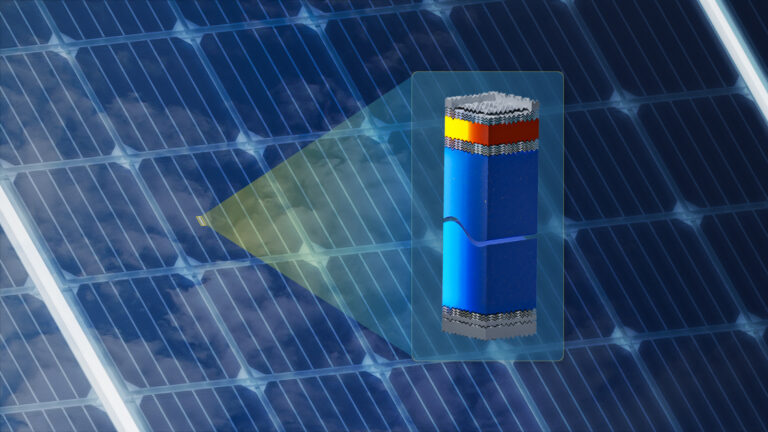
Lopatin’s high-resolution EELS technique has also assisted researchers from the KAUST Solar Center. One avenue of solar research is to develop low-cost solar materials based on organic polymers. To maximize the materials’ light capturing efficiency, solar researchers aim to combine different polymers or small molecules with complementary properties. But the performance gain depends on how well the two components mix, which has been very difficult to measure. “With both components made from carbon it is really difficult to distinguish one from another to tell whether they are well mixed,” Lopatin says.
However, one small difference between the components—their electronic properties—makes them suitable for EELS analysis, but only using the new technique.3 “Without it, the components are too similar and we don’t see the difference,” Lopatin says. “Using the extra resolution, I can see the electronic property difference in the two components and characterize how well they get mixed.”
These results enabled the solar team to identify the best methods for mixing the multicomponent organic solar cells.
High-resolution EELS is applicable to a wide range of materials and could provide new insights into many aspects of the electronic properties of materials. It represents just one of the innovations developed by experts in the KAUST Core Labs. Lopatin is not resting on his laurels, however. “I am developing a new method at the moment,” he says.
References
-
El-Demellawi, J.K., Lopatin, S., Yin, J., Mohammed, O.F., Alshareef, H.N. Tunable multipolar surface plasmons in 2D Ti3C2Tx MXene flakes. ACS Nano 12, 8485 (2018).| article
- Velusamy, D.B., El-Demellawi, J.K., El-Zohry, A.M., Giugni, A., Lopatin, S., Hedhili, M.N., Mansour, A.E., Di Fabrizio, E., Mohammed, O.F., Alshareef, H.N. MXenes for plasmonic photodetection. Advanced Materials 31, 1807658 (2019).| article
-
Liang, R.-Z., Babics, M., Savikhin, V., Zhang, W., Le Corre, V.M., Lopatin, S,. Kan, Z., Firdaus, Y., Liu, S., McCulloch, I., Toney, M.F., Beaujuge, P.M. Carrier transport and recombination in efficient “all‐small‐molecule” solar cells with the nonfullerene acceptor IDTBR. Advanced Energy Materials 8, 1800264 (2018).| article
ABOUT THE AUTHOR
Sergei Lopatin
Senior Scientist

You might also like

Applied Physics
Colorful solution to advanced disease diagnosis
Chemistry
Turning infrared solar photons into hydrogen fuel
Applied Physics
A single additive enables long-life, high-voltage sodium batteries

Bioengineering
Smart patch detects allergies before symptoms strike
Applied Physics
Two-dimensional altermagnets could power waste heat recovery
Applied Physics
Interface engineering unlocks efficient, stable solar cells
Applied Physics
The right salt supercharges battery lifespan

Applied Physics