Material Science and Engineering
A light touch for revealing atomic frameworks
Materials that normally become damaged inside electron microscopes can now be imaged with atom-scale resolution.


New algorithms based on geometric tricks and mathematical transformations enable high-resolution electron microscopes to quickly align and image materials, such as metal–organic frameworks, that are sensitive to beam damage.
© 2018 KAUST
To understand how atomic structure impacts biological function and chemical behavior, researchers often turn to high-resolution transmission electron microscopy (HRTEM). Many compounds, however, are too sensitive for these microscopes as powerful electron beams can knock out atoms or cause adverse heating. A team from KAUST has now developed a set of tools that can minimize beam damage in HRTEM using low doses of electrons.
Metal–organic frameworks (MOFs), with their sponge-like structure, are typical materials too delicate for HRTEM imaging. These compounds, with some of the highest surface areas ever recorded and customizable nanoscale pores, have enormous potential in gas storage and catalysis. But most MOFs breakdown during initial imaging stages when the microscope tries to align its beam with the crystal’s repeating zone axis.
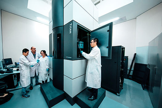
Daliang Zhang, Kun Li and colleagues from KAUST’s Imaging and Characterization Core Lab collaborated with Yu Han’s group in the University’s to find gentler ways of characterizing MOFs. Previously, the team has shown that special electron detection cameras can capture atom-scale-sized images using a low dose of a few electrons per pixel. However, this approach required sampling large numbers of randomly oriented MOFs to spot crystalline zones.
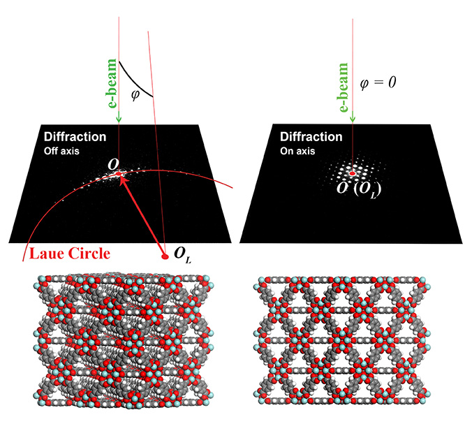
To make alignment simpler, the KAUST researchers developed a one-step procedure based on a parameter called the Laue circle that appears when electron beams encounter periodic structures. “Once we see a Laue circle, we know the crystal’s current orientation and the deviation angle from the desired position,” explains Zhang. “We can then align the crystal using a computer-controlled tilting process.”
Another problem is that beam-sensitive materials often move during electron microscopy imaging. To reduce this type of blurring, the team first took a series of short-exposure frames. Then, through a mathematical Fourier transform technique, they converted the image data of each pixel into a series of sine waves. Filtering out waves with weak amplitudes enabled the researchers to spot true periodic features and correct for image drift.
The researchers demonstrated the potential of their new HRTEM methods by resolving detailed features of aromatic rings and metal-exposed surfaces of a zirconium-based MOF, as well as subtle structural changes induced by heating. The resulting crystal-clear images may impact fields beyond MOFs as well.
“The expertise of the KAUST Core Labs was crucial for changing our HRTEM experiments from a trial-and-error process to one that is nearly routine,” says Han. “Now, we can study a number of delicate structures that are conventionally considered inexplorable, which is really exciting,” adds Zhang.
References
- Zhang, D., Zhu, Y., Liu, L., Ying, X., Hsiung, C.-E., Sougrant, R., Li, K. & Han, Y. Atomic-resolution transmission electron microscopy of electron beam–sensitive crystalline materials. Science 359, 675-679 (2018).| article
You might also like

Applied Physics
Colorful solution to advanced disease diagnosis

Chemistry
Turning infrared solar photons into hydrogen fuel

Applied Physics
A single additive enables long-life, high-voltage sodium batteries

Bioengineering
Smart patch detects allergies before symptoms strike

Applied Physics
Two-dimensional altermagnets could power waste heat recovery

Applied Physics
Interface engineering unlocks efficient, stable solar cells

Applied Physics
The right salt supercharges battery lifespan

Applied Physics