Electrical Engineering
Making waves for ultrahigh definition displays
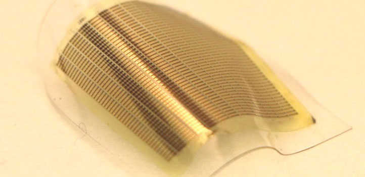
Wavy transistors that vertically gain width without increasing their on-chip footprint could drive future flexible displays.


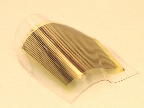
Wavy transistor arrays represent a step toward developing a single gadget with shape and size that can be dynamically reconfigured.
© 2017 Muhammad M. Hussain
Flexible ultrahigh resolution displays have benefits for next-generation mobile electronics, such as point-of-care medical diagnostic devices. KAUST has developed a unique transistor architecture that boosts the performance of the display circuitry.
Flat-panel displays implemented in smart watches, mobile devices and televisions rely on planar transistor circuits to achieve high-resolution and fast imaging. In these circuits, thin-film transistors, acting as switches, control the electric current that activates individual image elements, or pixels, consisting of light-emitting diodes (LEDs) or liquid crystals.
Future displays are expected to offer an even better visual experience through increases in resolution and frame rate. While transistor miniaturization can augment resolution, a higher field-effect mobility of the channel material can fulfill both these needs. It does this through its ability to facilitate electron and hole flows between contacts under applied voltage, which then allows transistors to switch faster and occupy a smaller pixel area.
To date, amorphous-oxide semiconductors, such as zinc oxide and indium-gallium zinc oxide, have provided transistor channels with modest mobility. Scaling down these transistors is expensive and introduces flaws known as short-channel effects that increase their power consumption and degrade their performance, explains Muhammad Hussain, who led the research team.
As an alternative, Hussain’s team has designed non-planar vertical semiconductor fin-like structures that are laterally interconnected to form wavy transistor arrays. The researchers opted for zinc oxide as the active channel material and generated the wavy architecture on a silicon substrate before transferring it onto a flexible soft polymer support using a low temperature process.
Thanks to the vertical orientation, the researchers widened the transistors by 70% without expanding their occupied pixel area, doubling the transistor performance. The wavy arrays exhibited reduced short-channel effects and higher turn-on voltage stability compared to their planar equivalents. Moreover, in a proof-of-concept experiment, they could drive flexible LEDs at twice the output power as their conventional counterparts. “The LEDs were brighter without increasing power consumption,” says Hussain.
According to Hussain, considering the transition from desktop to smart phone reveals an obvious trend: reduction in size and weight leads to better displays. Yet, most people juggle laptops, tablets and smart phones. “Having a single gadget with shape and size that can be dynamically reconfigured is a dream we are working toward,” he says. He notes that wavy transistor arrays represent a step in that direction.
References
- Hanna, A.N., Kutbee, A.T., Subedi, R.C., Ooi, B. & Hussain, M.M. Wavy architecture thin-film transistor for ultra-high resolution flexible displays. Small advance online publication, 13 November 2017.| article
You might also like

Bioengineering
Self-aware biosensors boost digital health monitoring

Bioengineering
Smart patch detects allergies before symptoms strike

Computer Science
Green quantum computing takes to the skies

Electrical Engineering
Micro-LEDs boost random number generation

Bioengineering
Sensing stress to keep plants safe

Computer Science
Sweat-sniffing sensor could make workouts smarter

Electrical Engineering
New tech detects dehydration by touching a screen

Electrical Engineering


