Material Science and Engineering
Clear leads to fully transparent devices
Large-area, two-dimensional semiconductors wired through transparent oxide conductors produce high-performance see-through electronics.


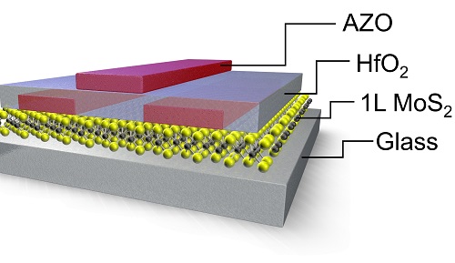
A fully transparent thin-film transistor consisting of a molybdenum sulphide (MoS2) monolayer; hafnium dioxide (HfO2), which is used for coating; and aluminum-doped zinc oxide (AZO) contacts.
© 2017 WILEY‐VCH Verlag GmbH & Co. KGaA, Weinheim
See-through electronic devices, such as transparent displays, smart windows and concealed circuits require completely translucent components if users are to digitally interact with their perceived surroundings and manipulate this information in real time. Now, KAUST researchers have devised a strategy that helps to integrate transparent conducting metal-oxide contacts with two-dimensional (2D) semiconductors into these devices.
Ultrathin semiconductor sheets that are composed of transition metals associated with chalcogen atoms, such as sulfur, selenium and tellurium, present exceptional electronic properties and optical transparency. However, to date, incorporating molybdenum sulphide (MoS2) monolayers into circuits has relied on silicon substrates and metal electrodes, such as gold and aluminum. The opacity of these materials has stalled attempts to develop fully transparent 2D electronic devices.
The KAUST team led by material scientists Xi-Xiang Zhang and Husam Alshareef has combined MoS2 monolayers with transparent contacts to generate a series of devices and circuits, such as transistors, inverters, rectifiers and sensors. The contacts consisted of aluminum-doped zinc oxide (AZO), a low-cost transparent and electrically conductive material that may soon replace the widely used indium-tin oxide. “We wanted to capitalize on the excellent electronic properties of 2D materials, while retaining full transparency in the circuits,” explains Alshareef.
According to Alshareef, the researchers grew the contacts over a large area by atomic-layer deposition, during which individual atom layers precisely accumulate on a substrate. Their main difficulty was to also form high-quality MoS2 monolayers on silicon-based substrates over a large area. “We overcame this by using an interfacial layer that promotes MoS2 growth,” says Alshareef.
The team also developed a water-based transfer process that moves the as-deposited large-area monolayers onto a different substrate, such as glass or plastic. The researchers then deposited the AZO contacts on the transferred 2D sheets before manufacturing the devices and circuits.
The resulting devices outperformed their equivalents equipped with opaque metal contacts, such as gate, source and drain electrodes, which demonstrates the high compatibility between transparent conducting metal-oxide contacts and MoS2 monolayers. “The transistors fabricated by the large-area process showed the lowest turn-on voltage of any reported MoS2 monolayer-based thin-film transistor grown by chemical vapor deposition,” says PhD student Zhenwei Wang, first author of the study.
“Additional circuits are planned that will help demonstrate that our approach is robust and scalable” says Alshareef.
References
-
Dai, Z., Wang, Z., He, X., Zhang, X.-X. & Alshareef, H. N. Large-area chemical vapor deposited MoS2 with transparent conducting oxide contacts toward fully transparent 2D electronics. Advanced Functional Materials 27, 1703119 (2017).| article
You might also like

Applied Physics
Colorful solution to advanced disease diagnosis

Chemistry
Turning infrared solar photons into hydrogen fuel

Applied Physics
A single additive enables long-life, high-voltage sodium batteries

Bioengineering
Smart patch detects allergies before symptoms strike

Applied Physics
Two-dimensional altermagnets could power waste heat recovery
Applied Physics
Interface engineering unlocks efficient, stable solar cells

Applied Physics
The right salt supercharges battery lifespan

Applied Physics