Material Science and Engineering
Atomically flat semiconductor devices
Perfect interfaces between sheets of two-dimensional semiconductors enable advanced electronic devices.


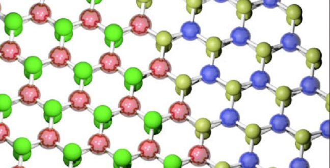

Two-step synthesis of two-dimensional nanosheets. The interface between the WSe2 and MoSe2 sheets is atomically perfect.
© 2015 KAUST
A method to grow atomically thin sheets of semiconductors to be used for two-dimensional electronic devices has been developed by researchers from KAUST1.
As silicon transistors approach the point beyond which they cannot be made smaller, alternative materials are needed for future electronic devices. This demand could be met however by two-dimensional semiconductor materials with the necessary fast electron transport capabilities and a thickness of the requisite atomic limit, such as graphene or transition metal dichalcogenides like WSe2 and MoS2.
Producing advanced electronic devices sheets of just one of these materials is not sufficient as it only allows for a limited functionality. More complex devices require the combination of different two-dimensional materials, ideally so that the different materials can transport first positive and then negative electrical charges across the device area. “It is fundamentally and technically important to integrate these two-dimensional layers to form devices and circuits in a monolayer lateral plane,” says Lain-Jong Li from KAUST’s Physical Science and Engineering Division who led the international research team.
Individually, two-dimensional semiconductors can already be fabricated with the right properties. The challenge lies in combining them into complex electronic devices because of difficulties in achieving a perfect interface at the junction where the different materials meet. Any imperfections at this interface may cause losses or inferior electrical or optical properties.
The researchers solved this problem by using a two-step growth technique where two-dimensional sheets are grown from atomic vapor inside a furnace. In the first step, a two-dimensional sheet of WSe2 is fabricated (see image). Then, MoS2 sheets are grown alongside the first WS2 layer using a second furnace at lower temperatures suited for MoS2.
The dedicated growth procedure optimized for each of the materials yields a sharp and functioning interface between the two sheets, indicated by high-resolution microscopy. The junction between the two materials operates like an electrical diode, and devices sizes of several micrometers have been achieved. Being semiconductors, the sheets also absorb light, and therefore operate as photodetectors and solar cells. In first tests, the required photovoltaic effect has been demonstrated.
Li says this achievement is only a first step. “There is still plenty of room for research into two-dimensional semiconductor sheets. For example, we are keen to know the possibility to use these junctions for energy harvesting, light emitting and optics, where more fundamental studies have to be done.”
References
- Li, M.-Y., Shi, Y., Cheng, C.C., Lu, L.-S., Lin, Y.C. et al. Epitaxial growth of a monolayer WSe2-MoS2 lateral p-n junction with an atomically sharp interface. Science 349, 524-528 (2015).| article
You might also like

Applied Physics
Colorful solution to advanced disease diagnosis

Chemistry
Turning infrared solar photons into hydrogen fuel
Applied Physics
A single additive enables long-life, high-voltage sodium batteries

Bioengineering
Smart patch detects allergies before symptoms strike
Applied Physics
Two-dimensional altermagnets could power waste heat recovery
Applied Physics
Interface engineering unlocks efficient, stable solar cells
Applied Physics
The right salt supercharges battery lifespan

Applied Physics