Material Science and Engineering
Snapshots help nanomaterials harvest light
Fleeting bursts of light and electrons reveal traps that hamper solar cells and sensors.


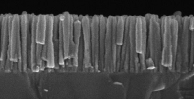
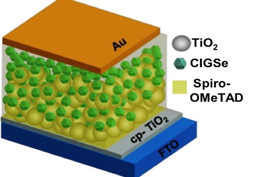
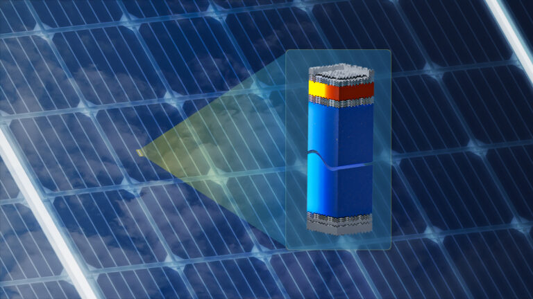
Image 1. A coating of zinc sulfide on copper indium gallium selenide (CIGSe) nanocrystals improves the efficiency of a photodetector in which the crystals are blended with materials (TiO2 and spiro-OMeTAD) that carry electrical charge to the device’s electrodes (Au and FTO).
Reproduced with permission from reference 2© 2016 American Chemical Society.
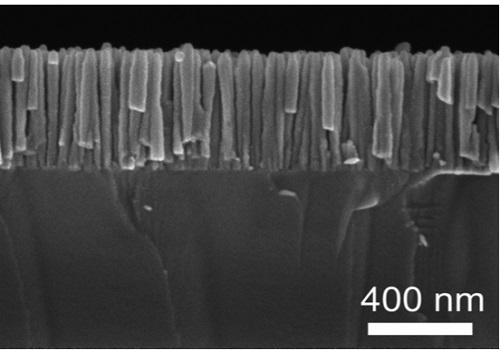
Image 2. Nanowires of indium gallium nitride (InGaN) on a silicon substrate can be used in applications such as laser diodes and photovoltaic devices.
© 2016 KAUST
Nanoscale materials are increasingly found in a variety of applications from sensors to solar cells, but these fragments of matter face a challenge from their own surface atoms, which often carry unpaired electrons. These act as trap states for other electrons, hampering the flow of charge and lowering the efficiency of devices. Until recently, there were no techniques to selectively study exactly how charge carriers interact with these surface trap states.
In 2010, researchers led by the late Nobel Prize winner Ahmed Zewail developed a four-dimensional scanning ultrafast electron microscope (4-D S-UEM)1, a technique to do just that.
Omar Mohammed, KAUST assistant professor of chemical science, was part of Zewail’s team, and he now leads a group at the KAUST Solar Center that investigates nanomaterials using 4-D S-UEM.
“The unique surface selectivity makes this technique highly sought in materials research,” he said. “The quality of a material’s surface holds the key to controlling its performance for almost every type of electronic and optoelectronic application.”
The 4-D S-UEM delivers brief pulses of laser light lasting no more than a few hundred femtoseconds (10-15 seconds or quadrillionths of a second). Some of that light is directed at the tip of a scanning electron microscope, where it generates bursts of just a few electrons at a time, and some of the light is focused on a sample to excite electrons within the material. When each burst hits the sample, it knocks some secondary electrons out of the upper two nanometers of the material, which can be measured by a detector.
“Images created by detecting secondary electrons essentially provide dynamical information selectively about the surface of the specimen,” said Mohammed.
By changing the time delay between optical and electron pulses and monitoring changes in the intensity of the secondary electrons, 4-D S-UEM can track the movement of electrons in the surface of the sample at the nanometer scale and capture events that take less than a picosecond (10-12 seconds) to occur.
Mohammed’s team recently used 4-D S-UEM to study nanocrystals of copper indium gallium selenide (CIGSe), a semiconductor being investigated for photovoltaic applications2. The researchers created thin films of CIGSe nanocrystals roughly 5 to 9 nanometers across and then compared their behavior with CIGSe nanocrystals that had a very thin coating of zinc sulfide. They found that this coating removed a significant proportion of the trap states from the surface of the nanocrystals.
When these shelled nanocrystals were used in a photodetector, the researchers found that it produced a much stronger signal, generating three times as much electrical current from incoming light. In photovoltaic devices, the shelled nanocrystals were twice as efficient at converting light into electrical power, with an efficiency of 2.62 percent.
The team has also investigated nanowires made from indium gallium nitride (InGaN), a material commonly used to produce blue light in light-emitting diodes (LEDs). Forming InGaN into nanowires can improve its performance in diverse applications such as laser diodes and photovoltaic devices.
However, energy loss within the wires reduces their efficiency. One explanation for this is that electrons are scattered by defects as they move through the material, and another is that surface traps rob excited electrons of their energy so that they recombine with the positive holes they left behind.
To settle the question, Mohammed’s team built a densely-packed array of vertical InGaN nanowires (with each measuring around 500 nanometers tall and 20 to 40 nanometers wide) on top of a silicon substrate. Using 4-D S-UEM, they studied the movement of electrons across the surface of the wires. The real-space imaging results suggest that the main cause of energy loss within the array comes from the recombination of electrons and holes at surface traps3.
“This information was not accessible before, and until very recently was a far–off dream,” said Mohammed.
Identifying this energy loss mechanism should help to design better strategies to minimize energy loss. Indeed, Mohammed’s group has already found that a coating of the carbon-based molecule octadecylthiol can remove surface traps in InGaN nanowires, preventing down electron-hole recombination and enhancing the efficiency of an LED.
These results demonstrate the power of the 4-D S-UEM technique, and the team is now investigating how charges move around the surfaces of other materials, including atom-thin sheets of semiconductors.
“In spite of this technique being relatively new, it has already been applied to study diverse phenomenon in photoactive materials commonly used in solar cell applications,” Mohammed noted.
References
- Mohammed, O. F., Yang, D-S., Pal, S. K. & Zewail, A. H. 4D scanning ultrafast electron microscopy: visualization of materials surface dynamics. Journal of the American Chemical Society 133, 7708-7711 (2011).| article
- Bose, R., Bera, A., Parida, M.R., Adhikari, A., Shaheen, B. S. et al. Real-space mapping of surface trap states in CIGSe nanocrystals using 4D electron microscopy. Nano Letters 16, 4417-4423 (2016).| article
- Bose, R., Sun,J., Khan, J.I., Shaheen, B.S., Adhikari, A. et al. Real-space visualization of energy loss and carrier diffusion in a semiconductor nanowire array using 4D electron microscopy. Advanced Materials 28, 5106–5111 (2016).| article
You might also like

Chemistry
Turning infrared solar photons into hydrogen fuel
Applied Physics
A single additive enables long-life, high-voltage sodium batteries

Bioengineering
Smart patch detects allergies before symptoms strike

Applied Physics
Two-dimensional altermagnets could power waste heat recovery
Applied Physics
Interface engineering unlocks efficient, stable solar cells

Applied Physics
The right salt supercharges battery lifespan

Applied Physics
Light-powered ‘smart vision’ memories take a leap forward

Applied Physics