Material Science and Engineering
Pumping perovskites into a semiconductor platform
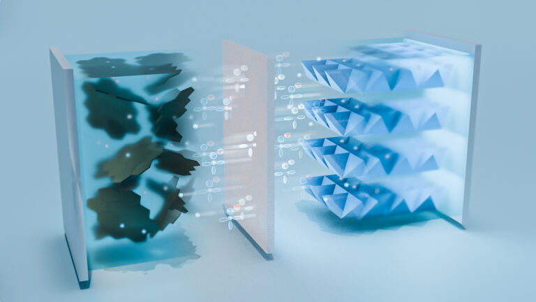
Fluid injection of perovskite semiconductors creates microwires to build different optoelectronic devices on a single silicon chip.


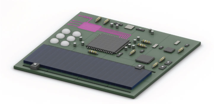
Materials called perovskites can be more readily incorporated into silicon-based semiconducting platforms by using a microfluidic pumping technology developed at KAUST.
The perovskites currently being explored for many applications in new technologies are diverse materials sharing the same crystalline structure as the natural mineral perovskite. These semiconducting materials show great promise in a variety of optoelectronic applications, such as light emitters, sensors and solar cells.
Compared to traditional semiconductors, perovskites are soft and unstable. “This makes it difficult to pattern them using standard lithography methods,” says materials scientist Iman Roqan at KAUST.
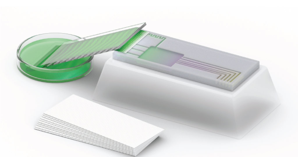
The team adapted microfluidic technologies to manipulate solutions carrying perovskites to create semiconducting microscale wires and then created the desired pattern of microchannels in a silicon wafer using a laser interference technique.
© 2021 KAUST; Heno Hwang
The challenge tackled by Roqan and her colleagues was to adapt microfluidic technologies to manipulate solutions carrying perovskites to create semiconducting microscale wires.
The first step in the procedure is to create the desired pattern of microchannels in a silicon wafer using a laser interference technique. The key innovation is to pump a solution containing perovskite ions into these microchannels, where the perovskite solidifies into the network of semiconductor wires.
“We are the first researchers to achieve this,” says Roqan, adding that the innovation, which has now been patented, will allow several different perovskite-based optoelectronic devices to be located on one silicon chip. For example, a single chip could embody a photodetector, transistor, light-emitting diode and a solar cell to act as the power supply.
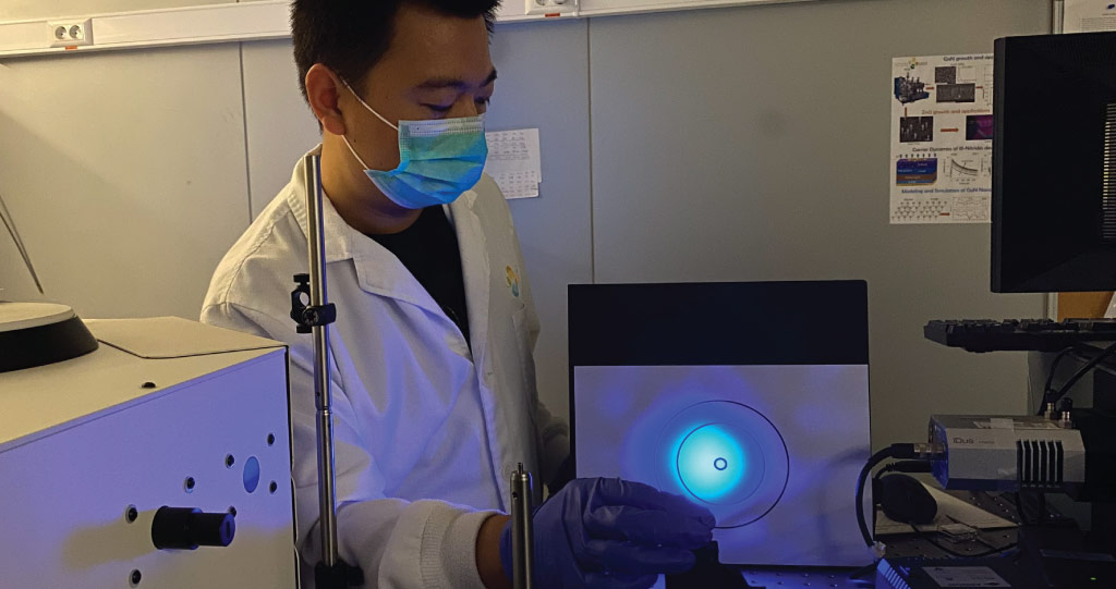
KAUST postdoc Bin Xin aligns the laser interference lithography systems used to create the array structures on the Si samples.
© 2021 KAUST
To demonstrate the potential of the technique, the team have built a high-performance photodetector.
“Unlike other options, our fabrication method is extremely simple and cost-effective, while avoiding creating waste materials,” Roqan says. Some metals used in perovskites are toxic, so avoiding their release into the environment is a significant advantage.
There remain challenges to overcome to advance from this initial proof-of-concept stage. For example, the team is working to bring the stability of the devices up to a standard suitable for large-scale industrial applications. Roqan expects that work currently in progress to achieve this is likely to lead to further patents, while also building more complex demonstration devices.
One of the most likely areas for commercial development is in the growing field of “lab on a chip” technology. This can combine processes such as sensing, signaling, microfluid manipulation and chemical separations and combinations to miniaturize many laboratory procedures used in medicine and biology. With miniaturization comes portability, potentially taking a full testing laboratory process out of the lab and into the outside world.
References
-
Xin, B., Pak, Y., Shi, M., Mitra, S., Zheng, X., Bakr, O.M. & Roqan, I.S. Micropump fluidic strategy for fabricating perovskite microwire array-based devices embedded in semiconductor platform. Cell Reports Physical Science 2, 100304 (2021).| article
ABOUT THE AUTHOR
Bin Xin
Postdoc
You might also like

Applied Physics
Colorful solution to advanced disease diagnosis

Chemistry
Turning infrared solar photons into hydrogen fuel
Applied Physics
A single additive enables long-life, high-voltage sodium batteries

Bioengineering
Smart patch detects allergies before symptoms strike

Applied Physics
Two-dimensional altermagnets could power waste heat recovery
Applied Physics
Interface engineering unlocks efficient, stable solar cells
Applied Physics
The right salt supercharges battery lifespan

Applied Physics