Electrical Engineering
Taking the heat out of emitters
Semiconductor light-emitting diodes fabricated on a metal substrate are less prone to overheating.


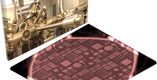
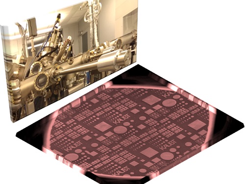
Molecular beam epitaxy (top left) creates integrated gallium-nitride optical devices on a metal substrate.
© 2016 KAUST
Micrometer-scale light emitters that can be incorporated into electronic chips could enable faster computation and communication systems in compact devices. Researchers at KAUST have developed a simple technique for fabricating optically active semiconductors on a metal substrate, showing that the devices work at room temperature and do not overheat.
The success of the modern electronics industry rests on the ability to fabricate thousands of electronic components on a single silicon chip. Optical devices could benefit in the same way from such an integrated-circuit approach, enabling a cheaper platform for optical communications or portable optical sensors. However, silicon is not the ideal material for optical applications, so an alternative material is required.
Chao Zhao, TienKhee Ng, Boon Ooi and colleagues from the Computer, Electrical and Mathematical Science and Engineering Division used the semiconductor gallium nitride to develop a platform for high-power light emission1.
“Nitride-based materials have been intensively studied for photonics applications such as solid-state lighting and displays because the alloys have direct bandgaps that cover the entire visible spectrum,” explained Zhao.
Gallium nitride-based structures have been created on silicon, sapphire and glass substrates. These materials are flawed, however, because they impair heat flow out of the device, causing a rise in temperature that eventually leads to malfunction.
The KAUST team fabricated gallium-nitride nanowires on a metal substrate instead; this substrate has better thermal properties. They started with a molybdenum substrate on which they laid down titanium and then titanium nitride using a technique called molecular beam epitaxy.
The light-emitting region itself was built up of alternating layers of gallium nitride and indium gallium nitride. This material self-assembled into vertical nanowires with diameters between 40 and 110 nanometers and 300 nanometers long. Each light-emitting diode incorporated many of these nanowires in a cylinder 200 micrometers across.
With better thermal properties than previously studied substrates, molybdenum can also act as the bottom electrical contact required to power the devices. This simplified the construction of the final devices.
The red light emitting diode worked at room temperature and exhibited no signs of overheating. For example, the researchers observed no drop in operation efficiency (known as thermal droop) as the current through the device increased. The emission color from the device also did not shift.
“Our work revolutionizes the semiconductor crystal growth technology and also realizes a practical platform for high-power nanowires light-emitters,” stated Zhao. “This uncovers new applications in high-power optoelectronics, high-speed and power electronics, display technology, energy conversion and green technologies.”
References
- Zhao, C., Ng, T. K., Wei, N., Prabaswara, A., Alias, M. S. et al. Facile formation of high-quality InGaN/GaN quantum-disks-in-nanowires on bulk-metal substrates for high-power light-emitters. Nano Letters 16, 1056−1063 (2016).| article
You might also like

Electrical Engineering
Laser security system protects online data

Electrical Engineering
Seeing smarter with a light-controlled synaptic device
Electrical Engineering
Gallium oxide electronics withstand extreme cold

Computer Science
AI-based hydrogen plant models improve power grid stability
Electrical Engineering
Quantum dot lasers outshine expectations

Bioengineering
Self-aware biosensors boost digital health monitoring

Bioengineering
Smart patch detects allergies before symptoms strike

Computer Science