Material Science and Engineering
Closing in on semiconductor band gaps
Atomically thin heterogeneous semiconductors with tunable electronic properties pave the way for next-generation two-dimensional devices.


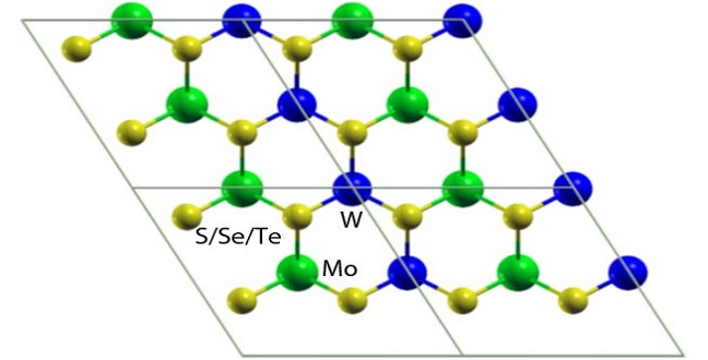
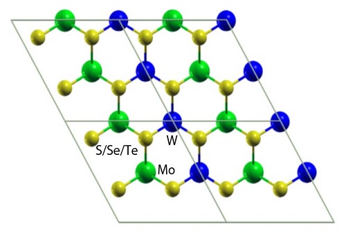
Atomistic models of laterally interfaced heterostructures.
Reproduced with permission from ref 1.© Physical Review B
The tunable electronic properties of atomically thin semiconductor sheets could lead to a wide range of materials with unprecedented electronic and optical uses, suggest new findings by researchers from KAUST1.
Semiconductors need to breach an intrinsic energy barrier known as band gap, which blocks electron flow through the material at low temperature. When exposed to heat or light, an electron in the semiconductor’s highest occupied energy level gains energy to reach the lowest unoccupied energy level, leaving a hole. This produces electrostatic pairs between negatively-charged electrons and positively-charged holes called electron-hole pairs.
Viable alternatives to silicon-based semiconductors are developed by combining molybdenum or tungsten with atoms from the chalcogen family, such as sulfur, selenium and tellurium. These are used for processes like photocatalysis and devices such as gas sensors and field-effect transistors. Unlike bulk substances, these transition metal dichalcogenide sheets generate electron–hole pairs with strong bonds — a prerequisite in optoelectronics.
To control the behavior of electron–hole pairs, scientists created mixed structures by vertically stacking or laterally interfacing molybdenum and tungsten dichalcogenide sheets. These are likely to produce materials that have new physical phenomena with diverse applications. However, their properties remained unclear, especially the nature of the band gap that separates the valence band maximum from the conduction band minimum.
To better understand these heterostructures, Udo Schwingenschlögl‘s team evaluated the structural, electronic, optical and photocatalytic properties of model sheets by atomic-scale computations.
“An accurate theoretical description of these materials requires rather sophisticated methods called hybrid functional calculations, which are computationally very demanding,” explained Schwingenschlögl.
Vertically stacked and laterally interfaced heterostructures displayed distinct band gaps depending on their layout. Specifically, layer-by-layer arrangements exhibited “indirect band gaps” with type-II band alignment.
This demonstrated that electron excitation has a multistep process. Also, valence band maximum and conduction band minimum spatially arose from different atomic layers, preventing the undesirable electron–hole recombination. Band gaps changed readily under mechanical strain. Besides new and dramatically different optical responses, the heterostructures showed strong solar light absorption, a bonus for photovoltaics.
“Our insights can guide the design of new tailor-made functional heterostructures for specific material requirements,” said Schwingenschlögl, noting the breadth of potential applications uncovered by the calculations.
The researchers are investigating the basic properties of the materials with a focus on their promising photocatalytic applications. They plan to assess their stability in water, a crucial aspect of photocatalysis, in addition to identifying potential interface problems with other substances, such as titanium dioxide and cadmium sulfide.
References
- Amin, B., Singh, N. & Schwingenschlögl, U. Heterostructures of transition metal dichalcogenides. Physical Review B 92, 075439 (2015). | article
You might also like

Applied Physics
Colorful solution to advanced disease diagnosis

Chemistry
Turning infrared solar photons into hydrogen fuel
Applied Physics
A single additive enables long-life, high-voltage sodium batteries

Bioengineering
Smart patch detects allergies before symptoms strike

Applied Physics
Two-dimensional altermagnets could power waste heat recovery

Applied Physics
Interface engineering unlocks efficient, stable solar cells
Applied Physics
The right salt supercharges battery lifespan

Applied Physics