Applied Physics
Nanoribbons carved into high-performance transistors
Extremely thin strips of phosphorus may help engineers to fabricate nanoscale transistors with atomically perfect structures.


Demand for ever-smaller computer chips is driving research into unconventional materials, such as graphene, that are only a single atom high. A new study predicts that another two-dimensional (2D) material, termed phosphorene, has the potential to find wide use in nanoelectronics due to its capacity to combine several transistor components into a single structure.
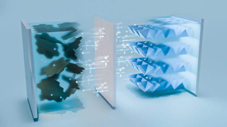
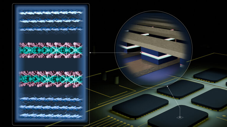
2D allotropes of black phosphorus (phosphorene) and blue phosphorus comprise a single layer of phosphorus atoms, connected together at angles that give them a rippled shape. Recent studies indicate that slicing these materials into long strips called nanoribbons could have intriguing effects. Depending on which direction the ribbons are cut, the compound can adopt either a zigzag or an armchair-like structure. While zigzag nanoribbons are metallic, the armchair version has semiconducting properties.
Enrique Montes and Udo Schwingenschlögl now propose a unique design for turning the nanoribbons into field-effect transistors that underpin modern circuitry. In these devices, current flows from a “source” to a “drain” electrode through a narrow semiconductor “channel.” When a third “gate” electrode is placed close to the channel, it can manipulate the current by switching it on or off, or by amplifying it.
Nanoscale field-effect transistors are challenging to fabricate, partly because electrical resistance at the contacts between the electrodes and the channel typically increases significantly as the size of the device shrinks. Montes and Schwingenschlögl investigated this problem using quantum-based simulations to characterize the electronic states of 2D phosphorus. These computations revealed that a transistor could fit on a single nanoribbon that sandwiched a semiconducting armchair-shaped portion between two metallic zigzag-shaped portions.
The team’s proposed nanoribbon, which is shaped like a “Z,” could be cut from a single sheet of the 2D material to have minimal contact resistance because of the atomically perfect interfaces between the electrodes and the channel. Simulations of the properties showed excellent switching and amplification performance. The transistor properties could also be tweaked by adding atoms, such as oxygen, to the edges of the nanoribbon.
“This setup has several advantages when it comes to engineering. It combines structural stability with a continuous junction that minimizes the contact resistance,” explains Montes. “And it can also be naturally integrated into circuit architectures.”
References
- Montes, E. & Schwingenschlögl, U. High-performance field-effect transistors Based on αP and βP. Advanced Materials 31, 1807810 (2019).| article
ABOUT THE AUTHOR
Enrique Montes
Alum

You might also like
Applied Physics
A single additive enables long-life, high-voltage sodium batteries
Applied Physics
Two-dimensional altermagnets could power waste heat recovery
Applied Physics
Interface engineering unlocks efficient, stable solar cells
Applied Physics
The right salt supercharges battery lifespan

Applied Physics
Light-powered ‘smart vision’ memories take a leap forward
Applied Physics
Natural polymer boosts solar cells
Applied Physics
2D materials could boost magnetic data storage

Applied Physics