Electrical Engineering
Conducting Fab lessons in a virtual clean room
A virtual platform makes learning how to fabricate a semiconductor device easier, safer and more interactive.


Place someone in a semiconductor fabrication laboratory for the first time, and they are unlikely to have the slightest idea where to start on the safe manufacturing of a device. Yet, these days, give most people these days a video game, and they’ll quickly figure out how to play.
KAUST electrical engineer Muhammad M. Hussain has been teaching a solid-state device laboratory course for the past 10 years. To improve the learning experience, Hussain designed vFabLab™, with the help of his former Ph.D. student, Galo Torres Sevilla, and an India-based virtual environment developer. vFabLab™ is a virtual clean room that provides an interactive environment for learning how to make semiconductor devices. Users are then better prepared to use the KAUST’s Nanofabrication Core Lab. “Users who have already trained on vFabLab™ immediately feel at home with the tools in the actual cleanroom. Training such users is more stimulating because they have already crossed the beginner stage and are now looking toward applying what they have learnt,” says Ahad Syed, one of the operational leads of the lab at KAUST.
“I was inspired by the fact that pilots are trained using flight simulators,” Hussain says. “Flying planes is a dangerous business. If that kind of task can be learned and executed using a simulator, why not have a simulator for the most expensive, hazardous educational training you can imagine?”
Clean rooms are laboratories with very tightly controlled levels of temperature, humidity and particulate matter. They are used in several industries, including pharmaceuticals and in the manufacture of the semiconductor devices used in most of today’s electronics. Clean room facilities are extremely expensive; prohibitively so for many educational institutions. They also involve the use of lasers and gases and have very strict safety protocols.
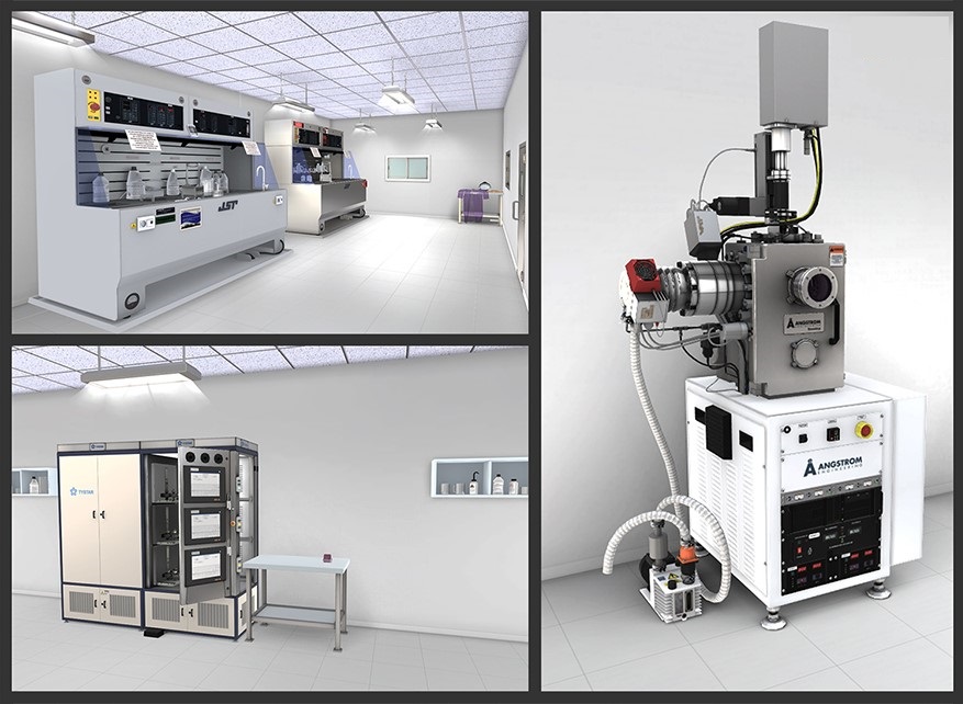
vFabLab™ provides learning opportunities for students whose universities don’t have clean rooms and for industries that want to train their personnel.
© 2019 Muhammad M. Hussain
“Having a virtual platform to teach students semiconductor device fabrication in a clean room greatly reduces the traffic inside real-world laboratories, as well as reducing safety hazards and expenses,” explains Hussain. “It also provides learning opportunities for students whose universities don’t have clean rooms, and for industries that want to train their personnel.”
vFabLab™ is an intuitive, free-to-use virtual environment. Once registered on the website, a process that requires administrator approval, users are shown a short video demonstrating how to use the platform. The user then chooses to start the first part of semiconductor manufacturing, a process called dry etching, and is guided through the task, step-by-step, using a computer interface and laboratory machine.
Once learned, the task can be attempted without guidance. If done well, they can answer questions to demonstrate that they’ve understood the process. This process can be repeated for the other steps of semiconductor manufacturing, giving users insight into the types of equipment and procedures necessary for each task.

This postdoc in Muhammad Hussain’s group is using the vFabLabTM online-based virtual environment in preparation for using the KAUST Nanofabrication Core Lab cleanroom facility.
© 2019 KAUST
“This is a great educational tool,” says Meyya Meyyappan, director of the Center of Nanotechnology at NASA’s Ames Research Center. “Anyone can sit at their desk and learn device fabrication end-to-end at their own pace. This tool is going to be well received all around the globe,” he adds.
Launched officially in January 2019, vFabLab™ is already incorporated into Hussain’s teaching. He says it is also being used in courses at Saudi Arabia’s King Fahd University of Petroleum and Minerals and at the Indian Institute of Science in Bengaluru. The website has approximately 250 individual registrants from 30 countries. Hussain will deliver a global webinar on vFabLab™, sponsored by the Institute of Electrical and Electronics Engineers (IEEE), on 24 April 2019.
vFabLab™ can be accessed across the world and is currently formatted for use on desktop computers and laptops, but there are plans to provide a mobile phone app version in late 2019.
References
- vFabLab can be accessed in Saudi Arabia from https://fablab.kaust.edu.sa/ and by the rest of the world at https://vfablab.org/
ABOUT THE AUTHOR
Gallo Torres Sevilla
You might also like

Electrical Engineering
Seeing smarter with a light-controlled synaptic device
Electrical Engineering
Gallium oxide electronics withstand extreme cold

Computer Science
AI-based hydrogen plant models improve power grid stability
Electrical Engineering
Quantum dot lasers outshine expectations
Bioengineering
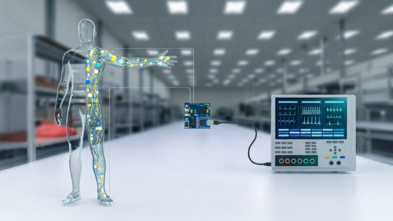
Self-aware biosensors boost digital health monitoring
Bioengineering
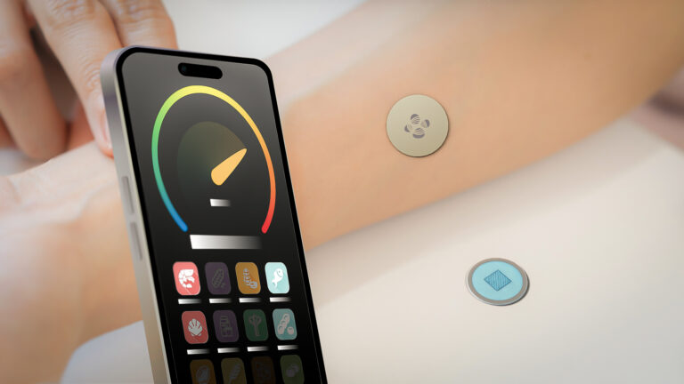
Smart patch detects allergies before symptoms strike

Computer Science
Green quantum computing takes to the skies
Electrical Engineering