Electrical Engineering
Silicon tubes for smarter transistors
Transistor designs based on nanotubes could considerably reduce the power demands of computers.


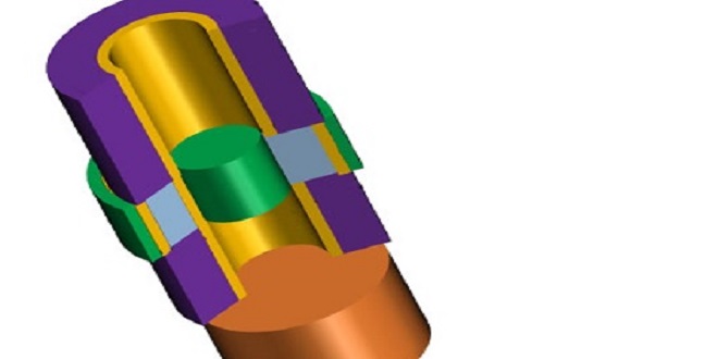
Contacted by a low-voltage source such as germanium (Ge), a silicon nanotube channel (light blue) is controlled by a gate architecture.
© 2015 KAUST
A new technology that can dramatically increase the integration of transistors on a computer chip whilst reducing its overall power consumption has been developed by researchers at KAUST1.
As more and more transistors are placed on computer chips the consumption of power per unit area is increasingly problematic. Under heavy computational loads chips can become very hot and demand cooling. The electrical power consumed by each transistor is related to the voltage applied as well as the current flowing through it. Reducing both amounts is crucial to advance future computer processors and the computer industry is working to bring power requirements down.
Three-dimensional transistor architectures — where transistors are made from thin nanoscale wires — are shown to reduce the voltage needed to control transistors. Another structure, nanoscale transistor architectures, based on quantum physical electron transport (so-called TFETs) instead of classical electrical currents, already helps to reduce the electrical current demand.
The KAUST researchers have studied TFETs based on nanowires in order to achieve a low overall power-consumption. In this architecture, a nanowire is used for electron transport, while an electrical contact is wrapped around the wire to turn the current on and off for the transistor control. Replacing this wire with a hollow silicon tube can reduce the current through the device (see image).
“Traditionally, physical electronics are designed to serve multi purposes. In our case, we have implemented design electronics based on specific needs. In this way it is easy for market penetration and to make tremendous impact,” says Muhammad Hussain from KAUST, who led the research team.
Using a semiconductor material with a low energy gap to supply the electrical charges to the tube will also reduce the voltage needed to operate this device. For the present design, the researchers considered silicon nanotubes where charges are supplied either by indium arsenide or germanium: both compounds have a lower energy gap than silicon.
The combination of new device architecture, along with the right choice of material, suggests that using a nanotube versus a nanowire can reduce electrical currents of such a transistor by up to a factor of five. These types of TFETs could therefore considerably reduce the energy requirements of future computer chips and enhance the integration density of transistors.
The next step will be to realize such devices, comments Hussain. “We have the capability in KAUST to grow these materials and are working toward that goal.”
References
- Hanna, A.N., Fahad, H.M. & Hussain, M.M. InAs/Si hetero-junction nanotube tunnel transistors. Scientific Reports 5, 9843 (2015).| article
You might also like

Electrical Engineering
Laser security system protects online data

Electrical Engineering
Seeing smarter with a light-controlled synaptic device

Electrical Engineering
Gallium oxide electronics withstand extreme cold

Computer Science
AI-based hydrogen plant models improve power grid stability

Electrical Engineering
Quantum dot lasers outshine expectations

Bioengineering
Self-aware biosensors boost digital health monitoring

Bioengineering
Smart patch detects allergies before symptoms strike

Computer Science