Electrical Engineering
Perfect absorption graphene style
A tiny device broadens the bandwith to enable absorption with wide-reaching potential for electrical engineering.


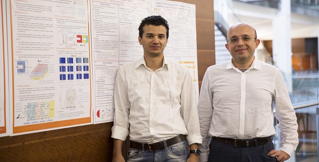
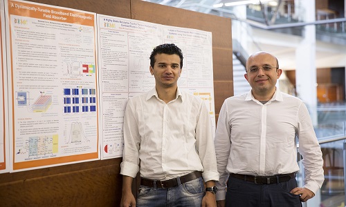
Mohamed Farhat (left) and Hakan Bagci from KAUST’s Division of Computer, Electrical, and Mathematical Sciences and Engineering.
© 2015 KAUST
A nanoscale near-perfect absorber, or ‘metascreen’, which operates at terahertz and infrared frequencies, has been developed by researchers at KAUST1. Using geometrically patterned graphene, coupled with a metal-backed ‘dielectric’ substrate, the new absorber will have broad application in electrical engineering, from communication networks to solar cell technology.
Graphene, a two-dimensional structure comprising carbon atoms arranged in a hexagonal lattice, has remarkable electronic properties such as high conductivity and stability. When combined with noble-metal nanostructures, graphene’s so-called ‘plasmon mode’ triggers the creation of coherent, tunable electron oscillations. These enable researchers to control — theoretically at least — the absorption of light at different frequencies.
“The quest for the ‘perfect’ absorber has been ongoing for some time,” says Mohamed Farhat, a member of the team led by Hakan Bagci of KAUST’s Division of Computer, Electrical, and Mathematical Sciences and Engineering, who worked on the project in collaboration with Pai-Yen Chen at Wayne State University, USA.
“The challenge is to find a material that can absorb significant electromagnetic energy, ideally 100 percent, which is present at different frequencies — for example in the light shining on solar cells,” explains Farhat. “Such absorbers would vastly improve the efficiency and sensitivity of these devices.”
The main problem with existing absorber designs is that they only operate on limited bandwidths, so not all the energy from multiple frequencies is absorbed.
Bagci and his team spent considerable time designing an absorber whose operative bandwidth would be maximized — aiming to utilize terahertz and infrared ranges.
Their absorber comprises a one-atom thick graphene sheet on a metal-backed dielectric substrate. The magnetic resonance of the substrate effectively widens the frequency range over which the graphene’s plasmon mode is sustained. The plasmon mode allows for the cancellation of magnetic fields reflected by the metallic background, widening the band of absorption.
The team used mathematical models to calculate the material properties of graphene and its response to different electromagnetic interactions. “We used extensive numerical simulations to verify our design, which can be optimized for given sets of geometry and substrate materials depending on the intended applications,” explains Farhat. ”The new absorber is simpler than previous designs and easier to fabricate.”
Near-perfect absorbers have numerous potential applications, from sensors and spatial light modulators, to energy harvesting, infrared camouflage and cloaking mechanisms. Farhat is confident the new design will make a major impact and hopes to work with experts in different fields to further expand the project.
References
- Chen, P-Y. Farhat, M. & Bagci, H. Graphene metascreen for designing compact infrared absorbers with enhanced bandwidth. Nanotechnology 26, 164002 (2015).| article
You might also like

Electrical Engineering
Laser security system protects online data

Electrical Engineering
Seeing smarter with a light-controlled synaptic device
Electrical Engineering
Gallium oxide electronics withstand extreme cold

Computer Science
AI-based hydrogen plant models improve power grid stability
Electrical Engineering
Quantum dot lasers outshine expectations

Bioengineering
Self-aware biosensors boost digital health monitoring
Bioengineering
Smart patch detects allergies before symptoms strike

Computer Science