Electrical Engineering
Nanoscale patterning is better with gas
Adding a gas enhances the processing of hybrid organic-inorganic materials for improved solar cells.
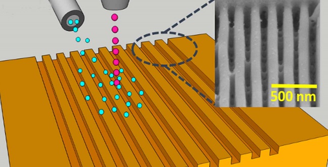
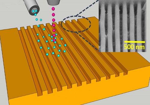
Adding aniodine or xenon difluoride gas aids nanoscale ion-beam etching of hybrid-perovskite materials.
© 2016 KAUST
A technique developed by KAUST scientists has made more controlled fabrication of optoelectronic devices produced from a hybrid of organic and inorganic materials possible.
Solar cells that are based on a perovskite material made by combining organic methylammonium ions with inorganic lead atoms plus a halide (chlorine, bromine or iodine) atom have already shown high efficiency and are economical to produce.
A drawback, however, is that is that the organic component is sensitive to the solvents and temperature changes that are often involved in device fabrication.
“Perovskite is a relatively new material, so fabrication technology is not well-developed,” said KAUST Professor of Electrical Engineering Boon Ooi. “Existing approaches are at the microscale and inhomogeneous.”
Ooi and his colleagues from the University’s Photonics Laboratory, the Imaging & Characterization Core Lab and the Solar & Photovoltaics Engineering Research Center have demonstrated a technique that can directly pattern perovskites with features smaller than one micrometer with little surface damage1.
Ooi’s team use focused-ion beam etching, a technique that involved firing gallium ions at CH3NH3PbBr3. The energy of these particles colliding with the sample caused the perovskite material to be ejected from the surface. To enhance this process, the team injected either gaseous xenon difluoride or iodine into the sample chamber during the etching process. These reacted with the perovskite to create volatile etch-products that were more easily removed.
By comparing samples etched with and without the injected gas, the team showed that the introduction of iodine almost doubled the etching rate over that with the gallium ions alone. The gas also made it easier to control the process, a key to making the devices reproducible.
The researchers also showed that the gas-assisted process resulted in less damage to the surface, as shown by the better optical properties of the material processed with both the iodine and xenon difluoride.
The researchers used their technique to create a grating, a series of equally spaced trenches. They were able to create trenches with a width as small as 120 nanometers separated by only 137 nanometers. Features of this size are important as they are smaller than the wavelength of the visible light emitted by these materials and thus enable construction of nanostructures that can manipulate light for better device performance.
“We are planning to implement the patterning directly on devices such as laser and solar cells to enhance their performance,” noted Ooi.
References
-
Alias, M. S., Yang, Y., Ng, T. K., Dursun, I., Shi, D. et al. Enhanced etching, surface damage recovery, and submicron patterning of hybrid perovskites using a chemically gas-assisted focused-ion beam for subwavelength grating photonic applications. The Journal of Physical Chemistry Letters 7, 137−142 (2016). | article
You might also like
Electrical Engineering
Gallium oxide electronics withstand extreme cold

Computer Science
AI-based hydrogen plant models improve power grid stability
Electrical Engineering
Quantum dot lasers outshine expectations
Bioengineering
Self-aware biosensors boost digital health monitoring

Bioengineering
Smart patch detects allergies before symptoms strike

Computer Science
Green quantum computing takes to the skies

Electrical Engineering
Micro-LEDs boost random number generation
Bioengineering


